Package structure for integrated circuit device and method of the same

Active Publication Date: 2009-10-29
MUTUAL PAK TECH
View PDF1 Cites 15 Cited by
  • Summary
  • Abstract
  • Description
  • Claims
  • Application Information

AI Technical Summary

Benefits of technology

[0005]In light of the foregoing, it is one object of the present invention to provide a w

Problems solved by technology

The conventional wafer level package process is only suitable for the circuits with larger size and less input/output devices.
Therefore, the con

Method used


Image

  • Package structure for integrated circuit device and method of the same
  • Package structure for integrated circuit device and method of the same
  • Package structure for integrated circuit device and method of the same

Examples


Embodiment Construction

[0018]The preferred embodiments of the present invention will now be described in greater details by referring to the drawings that accompany the present application. It should be noted that the features illustrated in the drawings are not necessarily drawn to scale. Descriptions of well-known components, materials, and process techniques are omitted so as not to unnecessarily obscure the features of the invention.

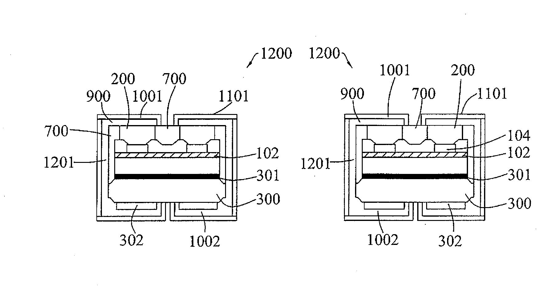
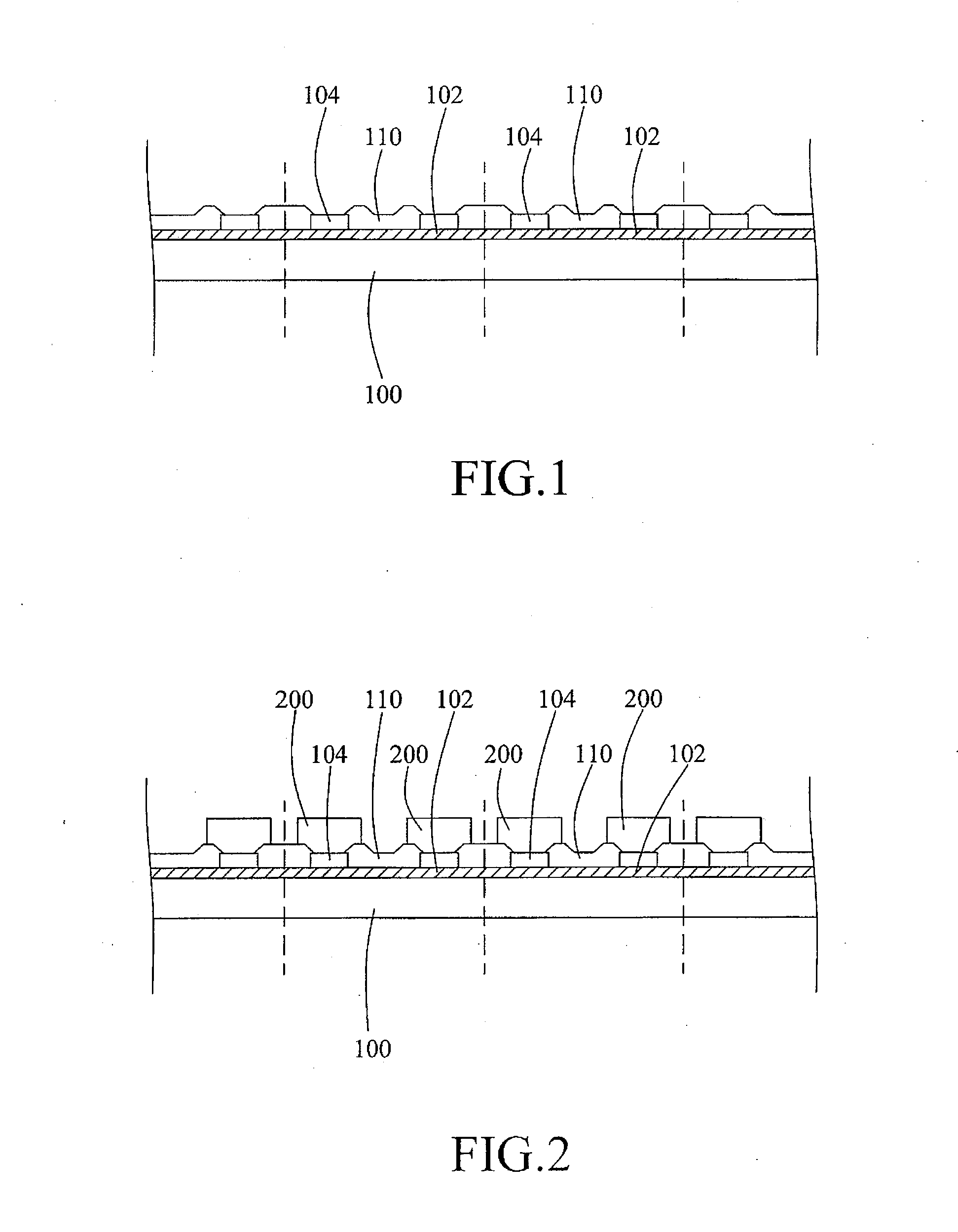
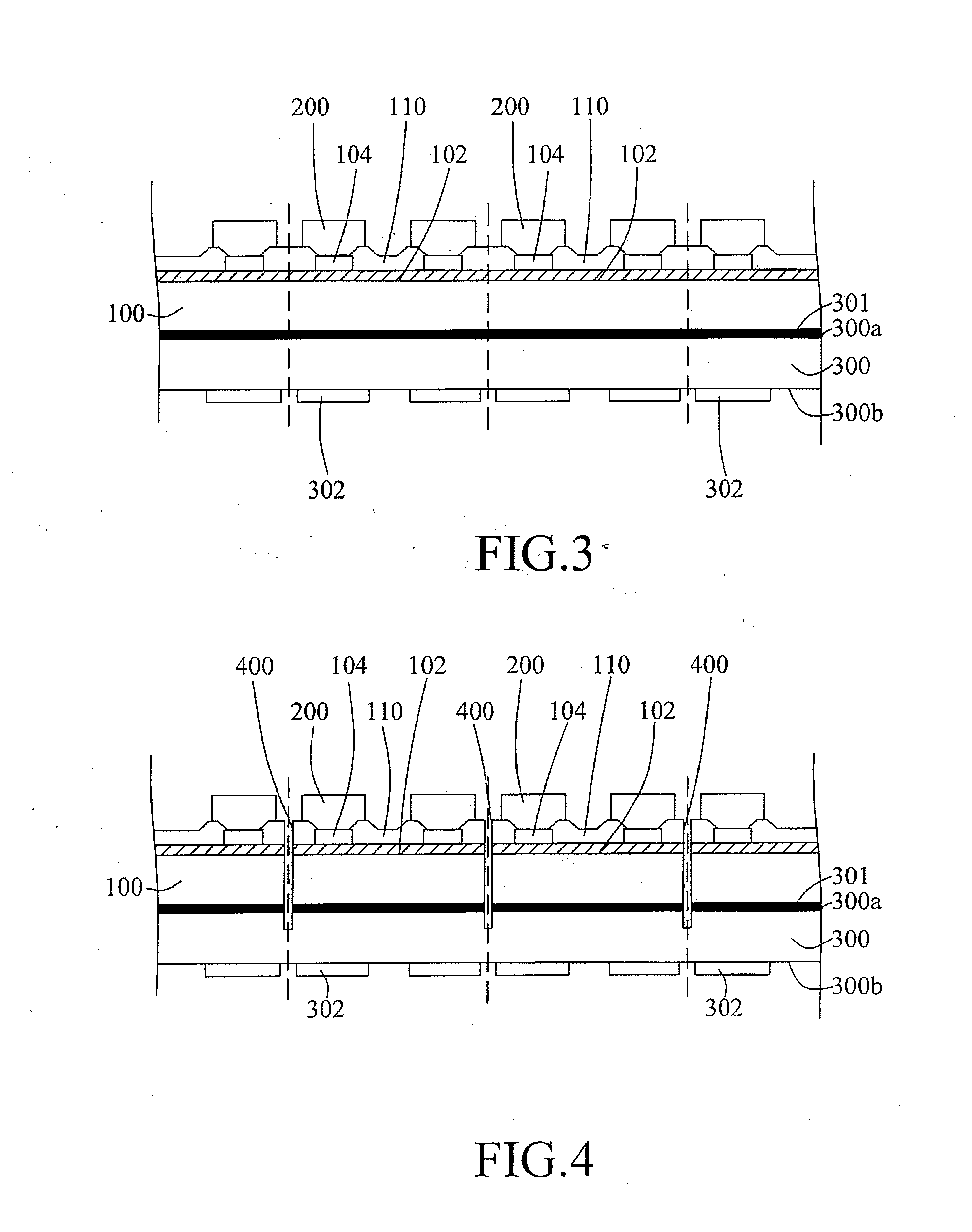
[0019]FIG. 1 to FIG. 12 are cross-sectional views illustrating a method of forming a package structure in accordance with an embodiment of the present invention. First, referring to FIG. 1, a wafer 100 is provided. The wafer 100 has a plurality of the integrated circuit devices 102, input / output contacts 104 formed on the integrated circuit devices 102, and a protective layer 110. The integrated circuit devices 102 can be a diode (such as a light-emitting diode, a photodiode, a laser diode, or a rectifier diode) or a transistor (such as MOS, CMOS, etc.). Since the pluralit...


PUM


Abstract

The present invention discloses a package structure for an integrated circuit device and method for manufacturing the same. The method includes providing a wafer with multiple integrated circuit devices; providing an extendable substrate having a first surface supporting the wafer; forming multiple anti-elongation layers on a second surface of the extendable substrate, the second surface being opposite to the first surface; forming multiple recesses in the wafer for separating the integrated circuit devices from each other; elongating the extendable substrate to enlarge the multiple recesses; and forming an insulating layer to fill the recesses and cover multiple integrated circuit devices.

Description

CROSS-REFERENCE TO RELATED APPLICATIONS[0001]This application claims priority to Taiwan Patent Application No. 97114993 entitled “PACKAGE STRUCTURE FOR INTEGRATED CIRCUIT DEVICE AND METHOD OF THE SAME,” filed on Apr. 24, 2008, which is incorporated herein by reference and assigned to the assignee herein.FIELD OF INVENTION[0002]This invention relates to a package structure for intergraded circuit devices and a method of the same, and more particularly, relates to a wafer level package structure for intergraded circuit devices and a method of the same.BACKGROUND OF THE INVENTION[0003]In a conventional wafer level package process, package structures are directly formed on a wafer which has circuits formed thereon by rerouting the wafer, coating the wafer with dielectric material, and attaching solder balls to the wafer. The conventional wafer level package process is only suitable for the circuits with larger size and less input / output devices. In detail, because the solder balls need ...

Claims


Application Information

Patent Timeline
IPC IPC(8): H01L23/498H01L21/50H01L21/768
CPCH01L21/561H01L2924/12041H01L23/14H01L23/3114H01L23/481H01L24/24H01L24/82H01L24/97H01L2221/68336H01L2221/68377H01L2224/13139H01L2224/13147H01L2224/16H01L2224/24226H01L2224/2518H01L2224/274H01L2224/82039H01L2224/82047H01L2224/97H01L2924/01002H01L2924/01013H01L2924/01029H01L2924/01047H01L2924/01078H01L2924/01079H01L2924/14H01L2924/3511H01L21/6835H01L2924/01033H01L2224/13111H01L2924/01006H01L2224/82H01L2924/12043H01L2924/00
Inventor HWAN, LU-CHEN
Owner MUTUAL PAK TECH
Why Eureka
Try Eureka