Strain Balanced Multiple Quantum Well Subcell In Inverted Metamorphic Multijunction Solar Cell

a solar cell and multi-junction technology, applied in the field of semiconductor devices, can solve the problems of presenting a number of practical difficulties, and the demand for solar cells to meet the needs of more sophisticated applications has not kept pace with demand

Inactive Publication Date: 2009-11-05
EMCORE SOLAR POWER
View PDF99 Cites 133 Cited by
  • Summary
  • Abstract
  • Description
  • Claims
  • Application Information

AI Technical Summary

Benefits of technology

[0029]In another aspect the present invention provides a solar cell comprising a first semiconductor substrate for the epitaxial growth of semiconductor material; a first subcell on the substrate including a first semiconductor material with a first band gap and a first lattice constant; a second subcell including a second semiconductor material with a second band gap and a second lattice constant, wherein the second band gap

Problems solved by technology

While significant progress has been made in this area, the requirement for solar cells to meet the needs of more sophisticated applications has not kept pace with demand.
The structures d

Method used


Image

  • Strain Balanced Multiple Quantum Well Subcell In Inverted Metamorphic Multijunction Solar Cell
  • Strain Balanced Multiple Quantum Well Subcell In Inverted Metamorphic Multijunction Solar Cell
  • Strain Balanced Multiple Quantum Well Subcell In Inverted Metamorphic Multijunction Solar Cell

Examples


second embodiment

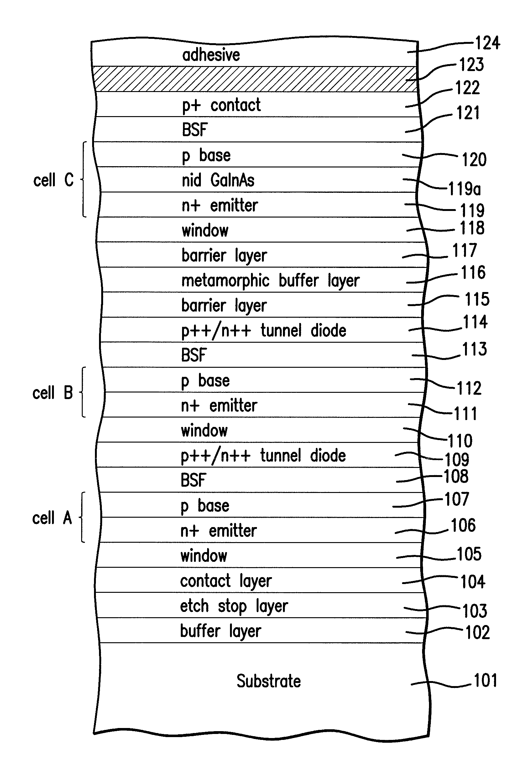
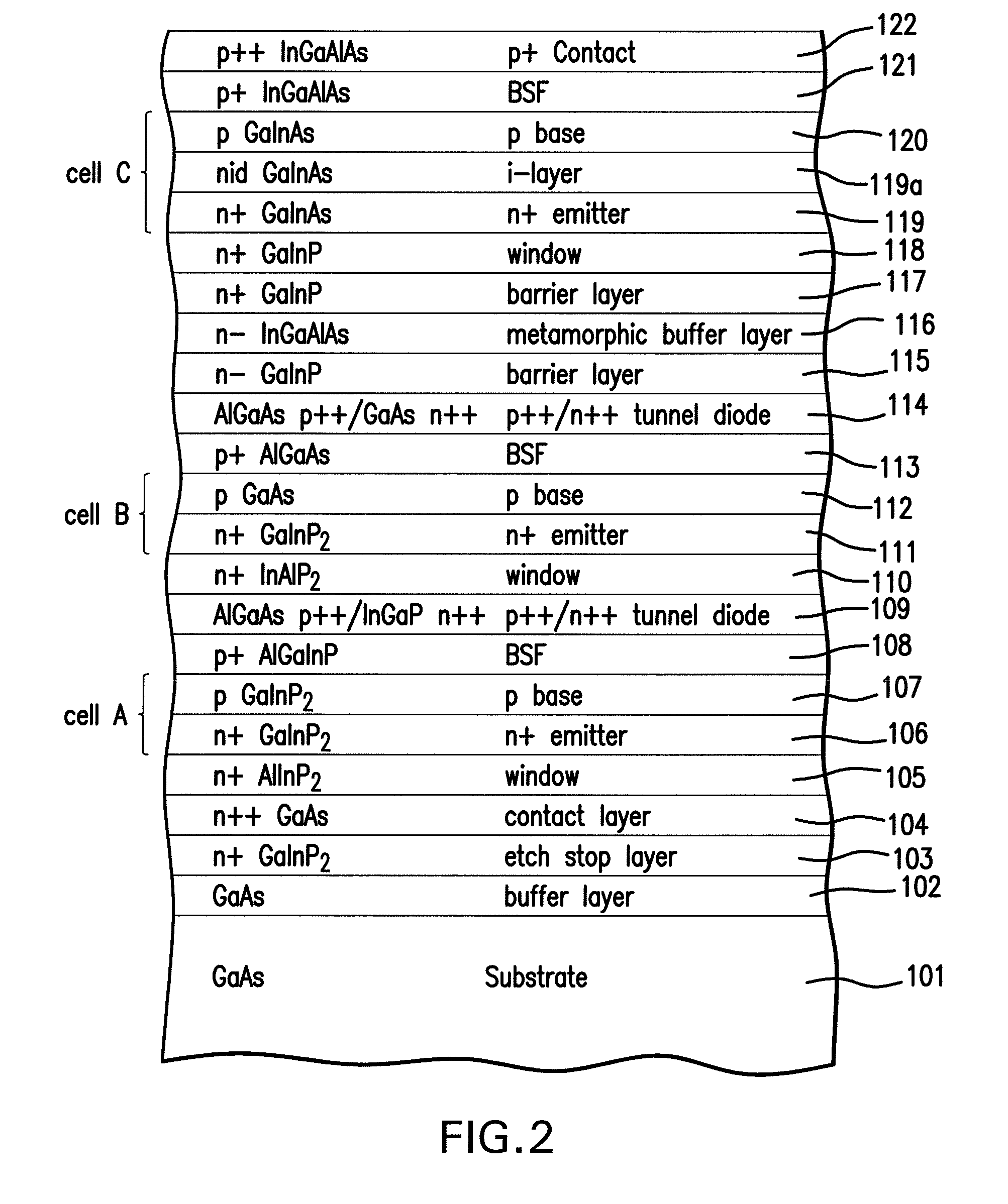
[0081]Although the preferred embodiment of the present invention utilizes a plurality of layers of InGaAlAs for the metamorphic layer 116 for reasons of manufacturability and radiation transparency, other embodiments of the present invention may utilize different material systems to achieve a change in lattice constant from subcell B to subcell C. Thus, the system of Wanlass using compositionally graded InGaP is the present invention. Other embodiments of the present invention may utilize continuously graded, as opposed to step graded, materials. More generally, the graded interlayer may be composed of any of the As, P, N, Sb based III-V compound semiconductors subject to the constraints of having the in-plane lattice parameter greater or equal to that of the second solar cell and less than or equal to that of the third solar cell, and having a bandgap energy greater than that of the second solar cell.

[0082]In another embodiment of the present invention, an optional second barrier l...

first embodiment

[0108]FIG. 14A is a cross-sectional view of the solar cell of FIG. 12 after the next process step in the present invention in which the surrogate substrate 125 is appropriately thinned to a relatively thin layer 125a, by grinding, lapping, or etching.

[0109]FIG. 14B is a cross-sectional view of the solar cell of FIG. 14A after the next process step in a second embodiment of the present invention in which a cover glass 513 is secured to the top of the cell by an adhesive. The cover glass 513 preferably covers the entire channel 510, but does not extend to channel 511.

[0110]FIG. 15 is a cross-sectional view of the solar cell of FIG. 14B after the next process step of the present invention in which the adhesive layer 124, the surrogate substrate 125 and the peripheral portion 512 of the wafer is entirely removed, leaving only the solar cell with the cover glass 513 on the top, and the metal contact layer 123 on the bottom, which forms the backside contact of the solar cell. The surrogat...


PUM


Abstract

A method of manufacturing a solar cell by providing a first semiconductor substrate for the epitaxial growth of semiconductor material; forming a first subcell on the substrate with a first semiconductor material with a first band gap and a first lattice constant; forming a second subcell with a second semiconductor material with a second band gap and a second lattice constant, wherein the second band gap is less than the first band gap and the second lattice constant is greater than the first lattice constant; the second subcell including a strain balanced quantum well structure; and forming a lattice constant transition material positioned between the first subcell and the second subcell, the lattice constant transition material having a lattice constant that changes gradually from the first lattice constant to the second lattice constant.

Description

REFERENCE TO RELATED APPLICATIONS[0001]This application is related to co-pending U.S. patent application Ser. No. 11 / 288,315 filed Apr. 18, 2007.[0002]This application is related to co-pending U.S. patent application Ser. No. 12 / 190,449 filed Aug. 12, 2008.[0003]This application is related to co-pending U.S. patent application Ser. No. 12 / 187,477 filed Aug. 7, 2008.[0004]This application is related to co-pending U.S. patent application Ser. No. 12 / 218,582 filed Jul. 18, 2008.[0005]This application is related to co-pending U.S. patent application Ser. No. 12 / 123,864 filed May 20, 2008.[0006]This application is related to co-pending U.S. patent application Ser. No. 12 / 102,550 filed Apr. 14, 2008.[0007]This application is related to co-pending U.S. patent application Ser. No. 12 / 047,842, and U.S. Ser. No. 12 / 047,944, filed Mar. 13, 2008.[0008]This application is related to co-pending U.S. patent application Ser. No. 12 / 023,772, filed Jan. 31, 2008.[0009]This application is related to c...

Claims


Application Information

Patent Timeline
IPC IPC(8): H01L31/0304H01L31/18
CPCH01L31/022425H01L31/03042H01L31/06875H01L31/0693Y02E10/544H01L31/0735H01L31/1844H01L31/1852H01L31/0725Y02P70/50
Inventor CORNFELD, ARTHUR
Owner EMCORE SOLAR POWER
Why Eureka
Try Eureka