Bond wire loop for high speed noise isolation

a noise isolation and bond wire technology, applied in the direction of electrical equipment, semiconductor devices, semiconductor/solid-state device details, etc., can solve the problems of increasing the number of electronic devices, increasing the complexity of devices, and increasing the number of conductors, so as to reduce coupling

Inactive Publication Date: 2009-11-05
MACOM TECH SOLUTIONS HLDG INC
View PDF5 Cites 7 Cited by
  • Summary
  • Abstract
  • Description
  • Claims
  • Application Information

AI Technical Summary

Benefits of technology

[0018]Also disclosed is a method for reducing coupling between package to die bonding wires comprising providing a package and a die. Then, electrically connecting the package to the die with two or more bonding wires, wherein a first bonding wire of the two or more bonding carries a signal and at least some of the signal couples into a second bond wire of the two or more bonding wires. The method also connects a first end of a dissipation wire to the package and connects a second end of the dissipation wire to the package or the die. As part of the connecting, the dissipation wire is between the first bonding wire and the second bonding wire to thereby shield the second bonding wire from signal coupling from the first bonding wire.

Problems solved by technology

As a result of the advancements in integrated circuit technology, the devices continues to grow more complex while the number of electronic devices on the integrated circuit and the number of conductors, i.e. bus width, that connect to the die increases.
As can be appreciated and seen in FIG. 1, in the area 136 near the die, the density of the bond wires 130 is high resulting in unwanted noise coupling between bond wires.
Thus, as a drawback to the prior art, an aggressor signal may couple into adjacent or even non-adjacent victim wire bond.
This coupling can be so significant that it limits data rates and can inhibit further die and package size reduction or density increases.
Prior art solutions also include increasing the distance between bond wires and expensive flip-chip solutions to minimize bond wire length.
Both of these proposed solutions are undesirable and costly.
By way of example, if supplying a supply voltage the operations within the circuit, such switching or other dynamic use of the supply voltage may create transients, which in turn cause unwanted noise coupling to victim bond wires.
In addition, the dissipation bond wire may have a path profile that matches the nearby signal bond wire generating noise energy.

Method used


Image

  • Bond wire loop for high speed noise isolation
  • Bond wire loop for high speed noise isolation
  • Bond wire loop for high speed noise isolation

Examples


Embodiment Construction

[0024]A grounded bond wire loop for high speed noise isolation in modern high speed IC package is disclosed. The noise coupling through package bond wire is increasingly becoming a challenge for high speed chip design. Disclosed in this specification is a solution to this difficult problem with minimum cost impact.

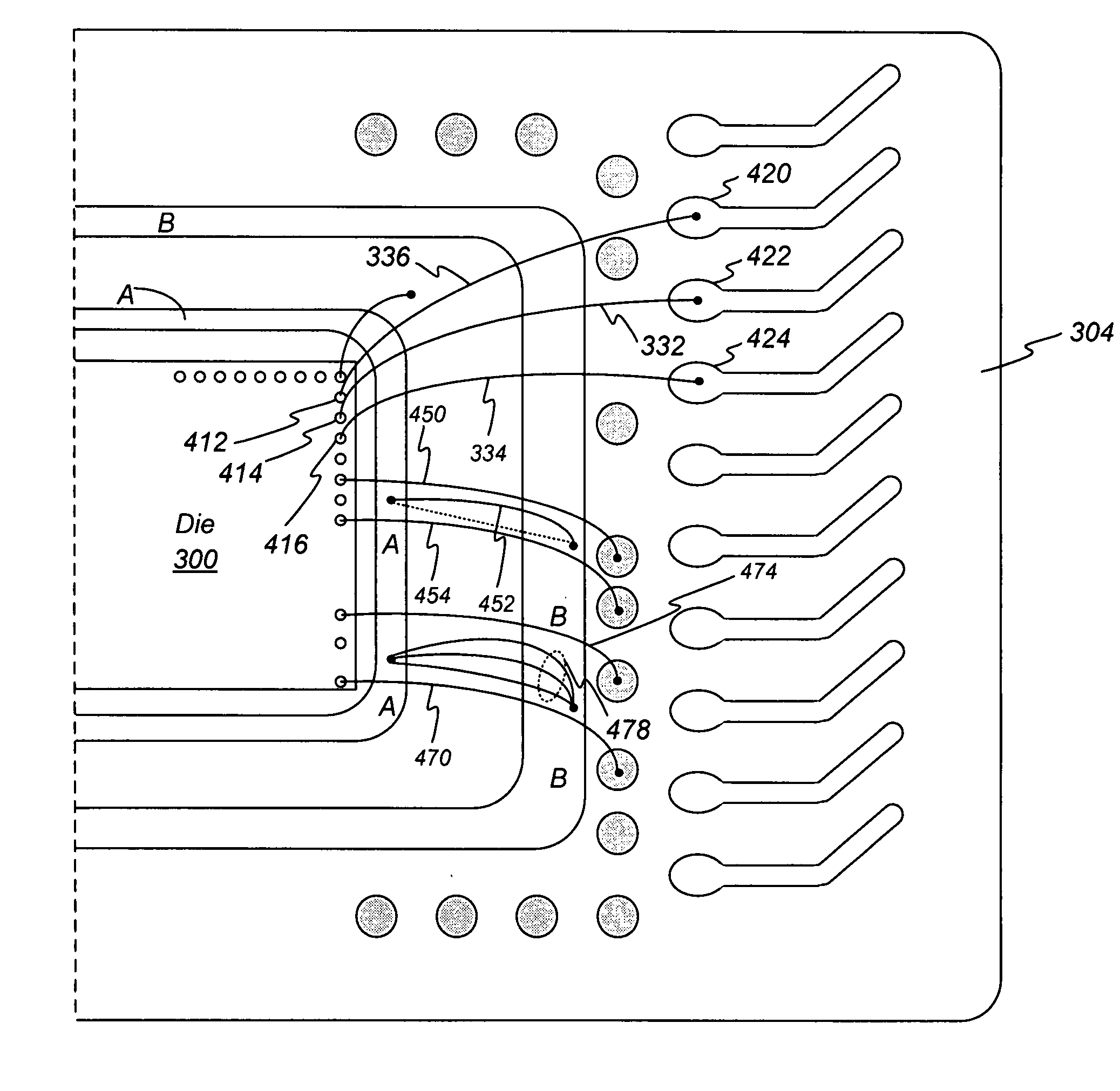
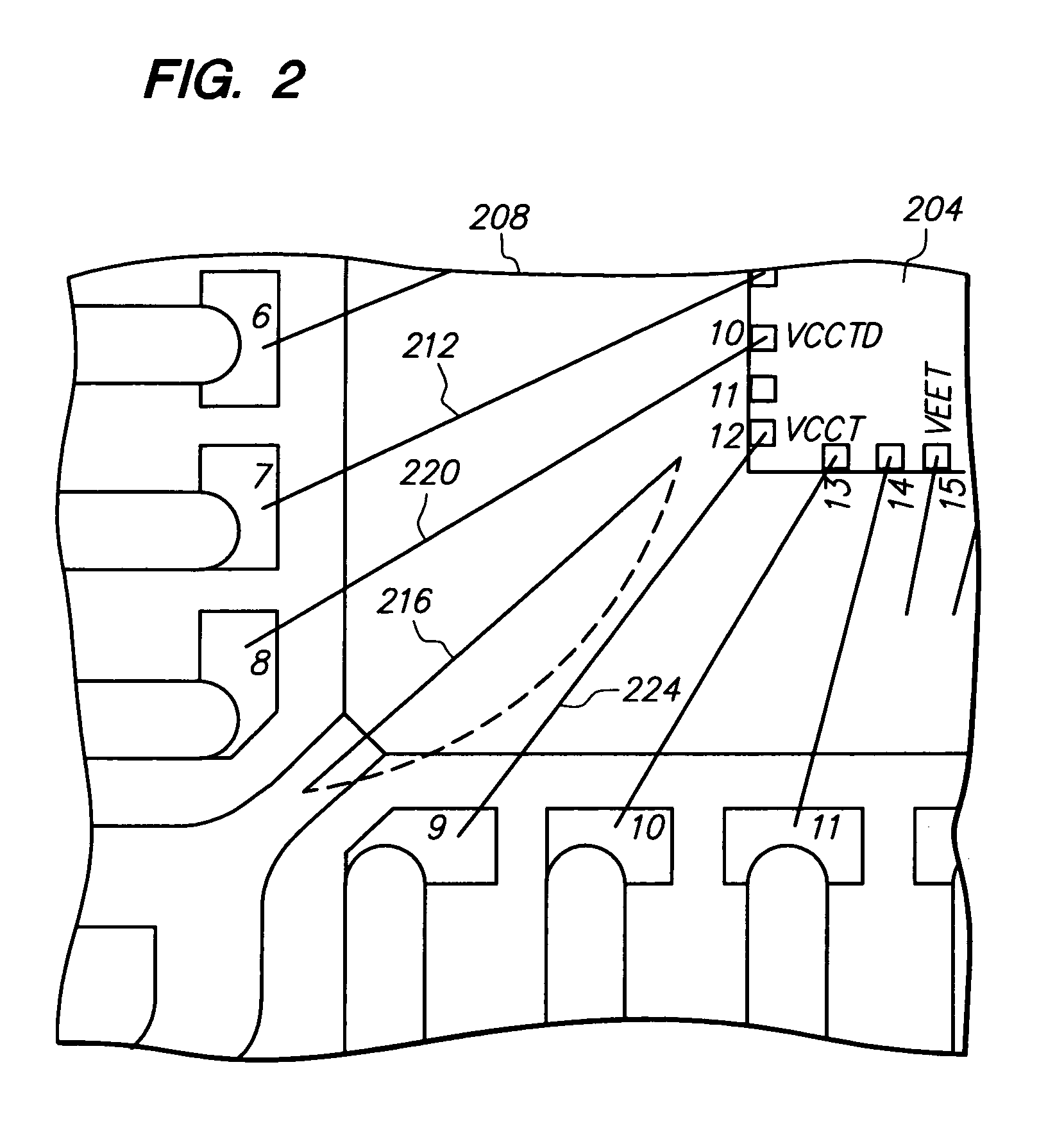
[0025]FIG. 2 illustrates a package 204 and die 208. Bonding wires 212 connect the die to the package. Disclosed herein is a bond wire loop 216 with both ends optionally grounded to form a very low impedance inductive loop. The loop may connect package to package as shown in FIG. 2 by the dissipation bond wire 216. The dissipation loop 216 is then inserted in between the bonding wires of two noisy and / or noise sensitive signals. The noise from any or both of the two signals will then couple to and short circuit in the grounded bond wire loop. The short circuit grounded loop (dissipation bond wire 216) will consume at least some of the noise energy before the noise energy re...


PUM


Abstract

Semiconductor dies embodying electronic circuits are enclosed and protected within a package. To electrically access the die, the package includes external electrical leads which in turn connect to internal bond wires. The bond wires electrically connect the package to the die. As die density and circuit complexity increase, bond wire are placed in greater proximity. As a result, signal coupling between adjacent bond wires also increases and this coupling reduces circuit performance and input/output rates. A dissipation bond wire is provided adjacent the signal or supply bond wire acting as an aggressor. The dissipation bond wire has a first end connecting to the package and the second end connecting to the die or the package to form a conductive loop which dissipates unwanted coupling from an aggressor bond wire before the coupling couples into victim bond wire. The dissipation bond wire may be grounded.

Description

PRIORITY CLAIM[0001]This application claims the benefit of and priority to U.S. Provisional Patent Application 61 / 125,972 filed Apr. 30, 2008 entitled Bond Wire Loop for High Speed Noise Isolation.FIELD OF THE INVENTION[0002]The invention relates to die packaging technology and in particular to a method and apparatus for noise isolation in bond wires.RELATED ART[0003]There exists a continuing demand for electronic devices that have greater functionality and speed. As such there has been, and continues to be, great strides in the development of new integrated circuit technologies that allow circuit designers to meet these needs. For example, electronic circuits increasingly operate at higher speeds and enjoy reductions in size as compared to circuits of a few years ago.[0004]By way of background, an integrated circuit is often referred to as an electronic “chip” and it often comprises numerous subparts. In particular, a die or integrated circuit, which contains or comprises one or mo...

Claims


Application Information

Patent Timeline
Patent Type & Authority Applications(United States)
IPC IPC(8): H01L23/49H01L23/488H01L21/60
CPCH01L23/552H01L24/48H01L2224/48233H01L2924/01033H01L2924/3025H01L2924/3011H01L2924/30107H01L2924/19107H01L24/49H01L2223/6611H01L2224/48091H01L2224/48227H01L2224/48237H01L2224/484H01L2224/49171H01L2224/4943H01L2924/01005H01L2924/01082H01L2924/014H01L2924/14H01L2924/00014H01L2924/00H01L2224/05554H01L2924/181H01L2224/49433H01L2224/45099H01L2224/05599H01L2924/00012
Inventor LI, XIAOMING
Owner MACOM TECH SOLUTIONS HLDG INC
Why Eureka
Try Eureka