Panel-shaped semiconductor module

a semiconductor module and panel-shaped technology, applied in the direction of solid-state devices, pv power plants, basic electric elements, etc., can solve the problems of uneven electric current distribution within solar battery cells, difficult to improve electric power generation efficiency, and difficulty in sufficiently increasing incident light usage rate, etc., to achieve simple structure, increase the efficiency of electric power generation or light emission output, and reduce the number of parts

Inactive Publication Date: 2009-11-12
SPHELAR POWER +1
View PDF25 Cites 2 Cited by
  • Summary
  • Abstract
  • Description
  • Claims
  • Application Information

AI Technical Summary

Benefits of technology

[0030]The granular semiconductor element has a base, another conductive layer formed on the surface of the base except for one end portion thereof and having a conductivity type different from that of the base, a pn junction, and first and second electrodes. The first and second electrodes are provided on the surface of the base on either side of the center thereof and ohmic-connected to the one end portion of the base and another conductive layer, respectively. Therefore, the sum of the distances from any point where carriers (electrons and holes) are generated to the first and second electrodes can be reduced throughout the semiconductor element, increasing the electric power generation or light emission output efficiency. Constituted by the inner metal case, the conductive connection mechanism electrically connecting multiple semiconductor elements can have a reduced number of parts and a simplified structure.
[0031]The conductive connection mechanism connects in parallel multiple semiconductor elements in each row and connects in series multiple semiconductor elements in each column. When some semiconductor elements fail for some reason, the current flows through an alternative path bypassing the failed semiconductor elements, whereby all normal semiconductor elements continue to work.
[0032]The inner metal case comprises multiple reflecting surface-forming grooves having a width decreasing from the opening to the bottom. Each reflecting surface-forming groove comprises a light reflecting bottom plate and a pair of light reflecting oblique plates. A corresponding row of multiple semiconductor elements is placed on a mount provided at the center portion of the bottom plate of the reflecting surface-forming groove. One of the first and second electrodes of the multiple semiconductor elements is electrically connected to the mount.
[0033]In this way, in the case of a light receiving semiconductor module, light collected by the reflecting surfaces of the reflecting surface-forming grooves can enter the semiconductor elements. The width of the reflecting surface-forming grooves can be three to four times larger or even much larger than the diameter of the semiconductor elements to increase the ratio of the reflecting surface-forming groove (light collection part) to the light receiving surface of the semiconductor elements, thereby increasing the light collecting magnification. In other words, a smaller number of semiconductor elements can effectively used to obtain high output power.
[0034]Furthermore, the semiconductor elements are placed on a mount protruding from the center portion of the bottom plate of the reflecting surface-forming groove. Light reflected by the bottom plate can enter the lower half of the semiconductor element.
[0035]Each row of multiple semiconductor elements is housed in each of multiple reflecting surface-forming grooves. Therefore, multiple cylindrical lenses corresponding to multiple reflecting surface-forming grooves, respectively, can advantageously used. The multiple reflecting surface-forming grooves formed by the inner metal case each comprises a bottom plate and a pair of oblique plates. The inner metal case can be constituted by a sheet of metal plate, reducing the number of parts and simplifying the structure.

Problems solved by technology

Therefore, it is difficult to sufficiently increase the incident light usage rate.
The solar battery cells have no electrode at the top, bottom, or either end and, therefore, the electric current distribution is uneven within a solar battery cell.
Hence, it is difficult to improve the electric power generation efficiency.
Furthermore, all solar battery cells mounted on the sheet are connected in parallel, which is inconvenient for increasing the output voltage of the solar battery module.
This causes a drawback that the distance between the upper half light receiving surface and the positive and negative electrodes of a spherical solar battery cell is large and the resistance loss upon output electric current retrieval is increased.
Furthermore, all solar battery cells of the solar battery module are connected in parallel, which is inconvenient for increasing the output voltage of the solar battery module.

Method used


Image

  • Panel-shaped semiconductor module
  • Panel-shaped semiconductor module
  • Panel-shaped semiconductor module

Examples


embodiment 1

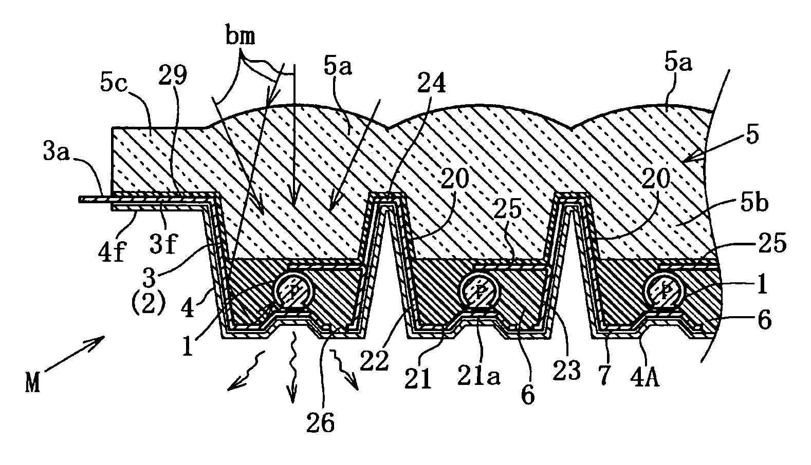
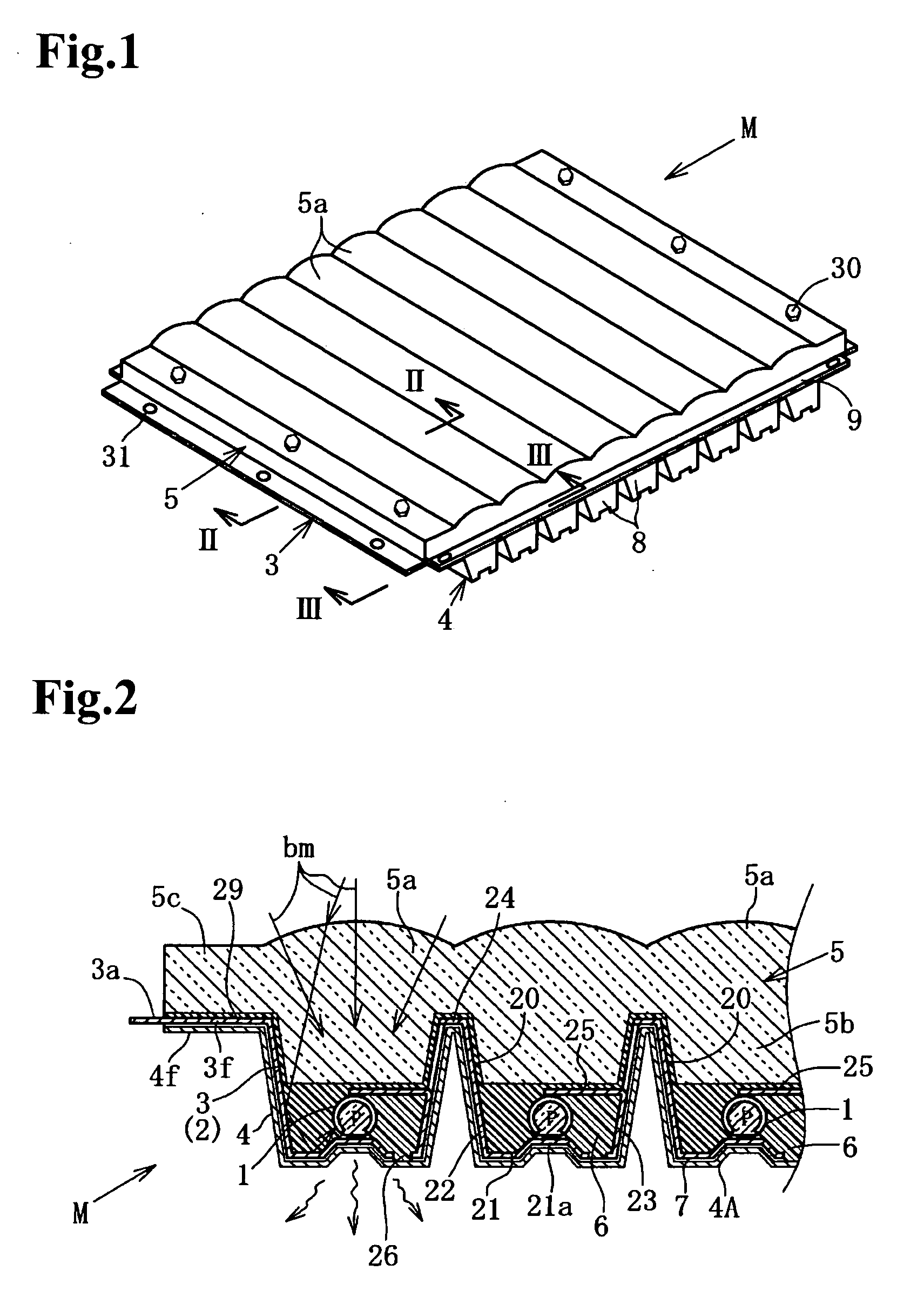
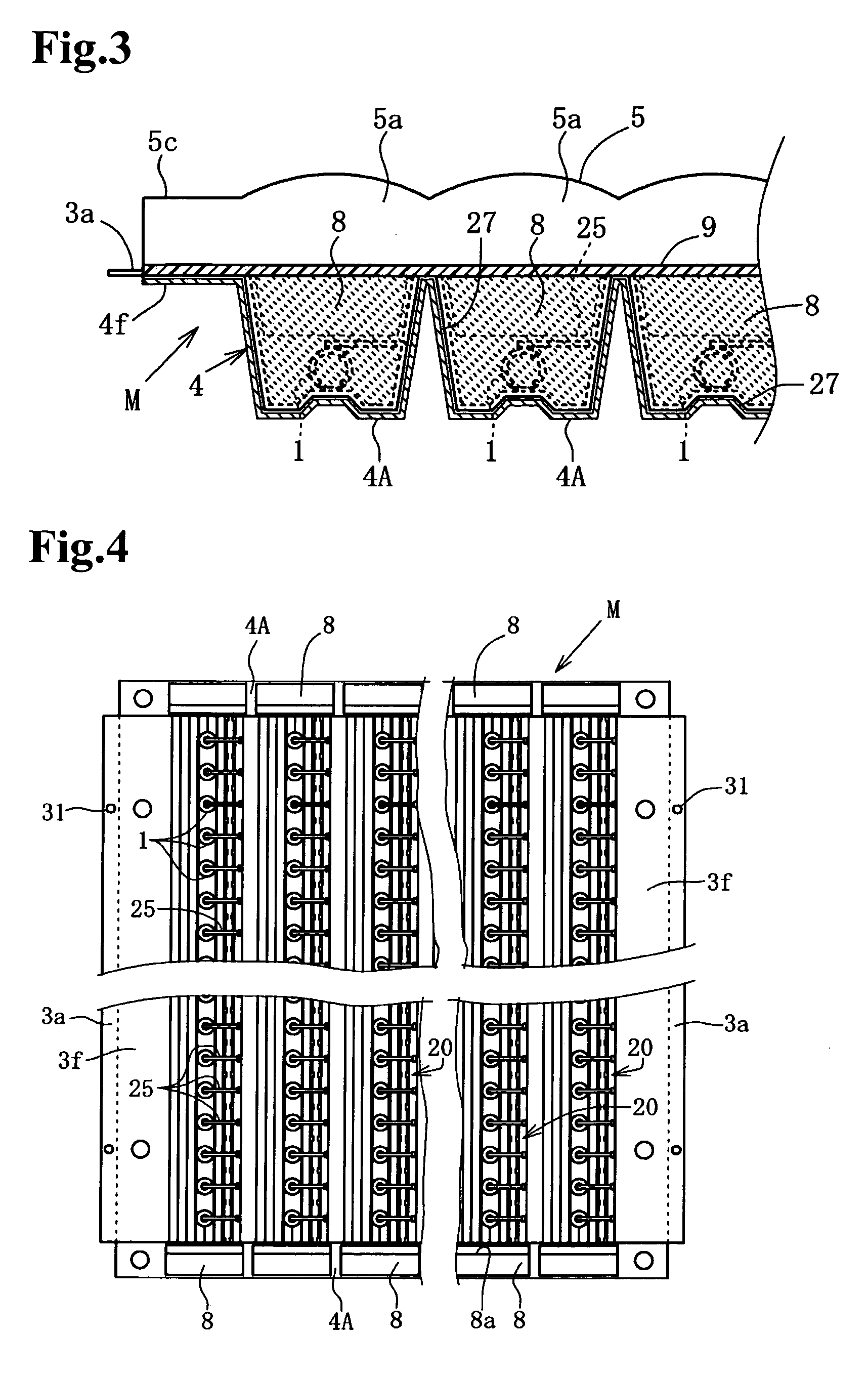
[0093]The panel-shaped semiconductor module relating to Embodiment 1 is a solar battery module (solar battery panel) receiving the sunlight and generating electric power. This solar battery module M will be described with reference to the drawings. As illustrated in FIGS. 1 to 5, the solar battery module M comprises multiple granular semiconductor elements 1 having light receiving capability, a conductive connection mechanism 2 electrically connecting the semiconductor elements 1 (see FIG. 9), an inner metal case 3 housing the multiple semiconductor elements 1, an outer metal case 4 fitted on the underside of the inner metal case 3, a transparent cover member 5 covering the top of the inner metal case 3, a silicone rubber insulating synthetic resin material 6 introduced in the inner metal case 3, a synthetic resin layer 7 bonding the inner and outer metal cases 3 and 4 together, multiple side plug blocks 8, and two reinforcement plates 9.

[0094]As illustrated in FIG. 8, the semicondu...

embodiment 2

[0132]A solar battery module Ma (panel-shaped semiconductor module) illustrated in FIG. 11 has a duct member 35 fitted on the underside of the above described solar battery M. The solar battery module Ma has the same structure as the solar battery module M except for the duct member 35. Therefore, the same components are designated by the same reference numerals and their explanation will be omitted. The duct member 35 has an inverted trapezoidal body 35a forming a coolant passage 36 together with the outer metal case 4 for a forced or natural flow of a coolant fluid such as air and cooling water, and flanges 35f extending from right and left ends of the body 35a. The flanges 35f are each fastened to the flat plate 5c of the cover member 5, flange 3f of the inner metal case 3, and flange 4f of the outer metal case 4 by multiple bolts 30 from below.

[0133]With a coolant such as air and cooling water running through the coolant passage 36, the inner and outer metal cases 3 and 4 and se...

embodiment 3

[0134]This embodiment relates to light emitting semiconductor elements (light emitting diodes) applied to a high output power light emitting diode module with a reflecting mechanism, which is a panel-shaped semiconductor module. This light emitting diode module with a reflecting mechanism comprises light emitting semiconductor elements in place of the semiconductor elements 1 of the above described solar battery module M.

[0135]The light emitting semiconductor element will be described hereafter.

[0136]As illustrated in FIG. 12, a light emitting semiconductor element 40 has a nearly spherical (a partial sphere close to a sphere) base 41 consisting of an n-type semiconductor crystal, a p-type diffusion layer 42 formed in the surface part of the base 41 (which corresponds to another conductive layer having a conductivity type different from the base), a nearly spherical pn junction 43 formed by the base 41 and diffusion layer 42, positive and negative electrodes 44 and 45, and an antire...


PUM


Abstract

A solar battery module as a panel-shaped semiconductor module comprises multiple spherical or nearly spherical, granular electric power generation semiconductor elements arranged in multiple rows and columns, a conductive connection mechanism electrically connecting in parallel multiple semiconductor elements in each row and connecting in series multiple semiconductor elements in each column, and a conductive inner metal case housing the multiple semiconductor elements and constituting the conductive connection mechanism, wherein each row of semiconductor elements is housed in each reflecting surface-forming groove of the inner metal case, the positive electrodes of the semiconductor electrodes are connected to the bottom plate and the negative electrodes are connected to finger leads, the bottom plate of each reflecting surface-forming grove has a cutoff slit, and the top is covered with a transparent cover member.

Description

TECHNICAL FIELD[0001]The present invention relates to a panel-shaped light receiving or emitting semiconductor module and particularly to a semiconductor module comprising multiple granular semiconductor elements (semiconductor devices).BACKGROUND TECHNOLOGY[0002]A variety of solar batteries (solar battery modules and solar battery panels) comprising external lenses for yielding large output power by means of a small light receiving area have been proposed. However, because the larger areas are realized in silicon solar batteries and production cost of solar battery cells and solar battery modules is reduced, light collection by external lenses is less used.[0003]On the other hand, in the solar battery using expensive compound semiconductors such as gallium arsenide (GaAs), light collection by external lenses is assumed to be economical and proposed in many documents.[0004]The U.S. Pat. No. 4,136,436 and the U.S. Pat. No. 6,204,545 by the inventor of the present application propose ...

Claims


Application Information

Patent Timeline
Patent Type & Authority Applications(United States)
IPC IPC(8): H01L31/052H01L33/00H01L33/48H01L31/04
CPCH01L31/035281H01L31/048H01L31/0543H01L31/0508H01L31/0521Y02E10/52
Inventor NAKATA, JOSUKE
Owner SPHELAR POWER
Why Eureka
Try Eureka