Light-emitting diode and method for fabrication thereof

a technology of light-emitting diodes and transparent substrates, which is applied in the direction of semiconductor/solid-state device manufacturing, electrical apparatus, semiconductor devices, etc., can solve the problems of not studying the exoergic property, lowering the light-emitting efficiency and degrading brightness, and failing to optimize the electrode disposition. , to achieve the effect of high exoergic property, high degree of electric current, and high brightness

Inactive Publication Date: 2009-11-12
SHOWA DENKO KK
View PDF4 Cites 44 Cited by
  • Summary
  • Abstract
  • Description
  • Claims
  • Application Information

AI Technical Summary

Benefits of technology

[0045]According to this invention described above, since a transparent-substrate light-emitting diode possessing a light-emitting layer made of a compound semiconductor has the relation of the area of the light-emitting layer and the area of the back surface of the transparent substrate and the condition of the side face of the transparent substrate optimized, it is made possible to provide a light-emitting diode that possesses such high brightness as has never been attained heretofore, exhibits a high exoergic property and suits use of a high degree of electric current.
[0046]Further, according to this invention, the transparent-substrate light-emitting diode possessing a light-emitting layer made of a compound semiconductor is enabled to have the disposition of electrodes and the shape of chips optimized. This invention, therefore, is capable of providing a light-emitting diode that has the efficiency of extracting light from the light-emitting part enhanced to a level not attainable heretofore, exhibits high brightness, suppresses the operation voltage and possesses high reliability.

Problems solved by technology

The conventional technique has proposed numerous shapes for devices so configured as to have electrodes formed each on the first surface and the back surface of a light-emitting diode but has not studied the exoergic property exhibited by such a device when the device is used with an electric current of high level.
It is known that the deficiency of the exoergic property results in elevating the temperature of the light-emitting layer, lowering the light-emitting efficiency and degrading the brightness.
The structure of the device using a transparent-substrate AlGaInP light-emitting layer and having two electrodes formed on a light-extracting surface entails such problems as complicating the shape, failing to optimize the electrode disposition, the side face condition and the back surfaces of the light-emitting layer and device and not acquiring high brightness and sufficient exoergic property.
When the light-emitting layer is made smaller and the area of the back surface is made larger for the purpose of enhancing the exoergic property, the problem of cost ensues because the expensive light-emitting layer incurs a great loss.

Method used


Image

  • Light-emitting diode and method for fabrication thereof
  • Light-emitting diode and method for fabrication thereof
  • Light-emitting diode and method for fabrication thereof

Examples


example 1

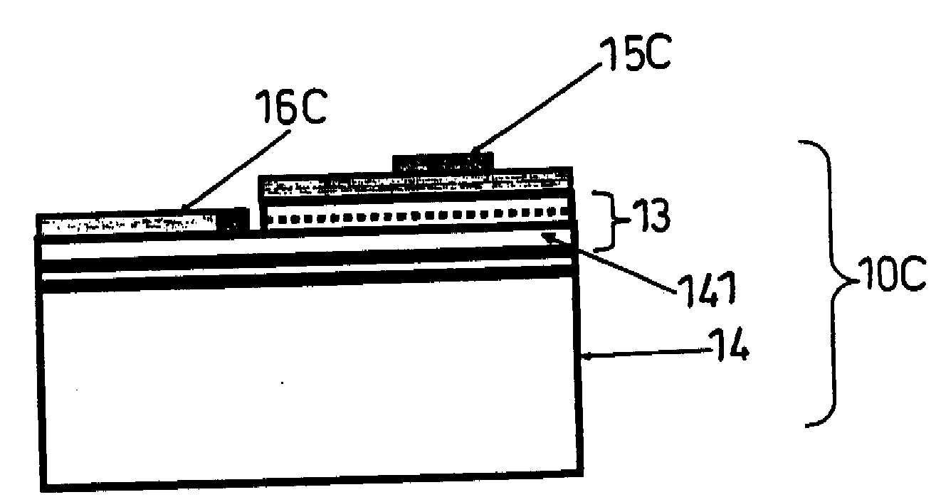
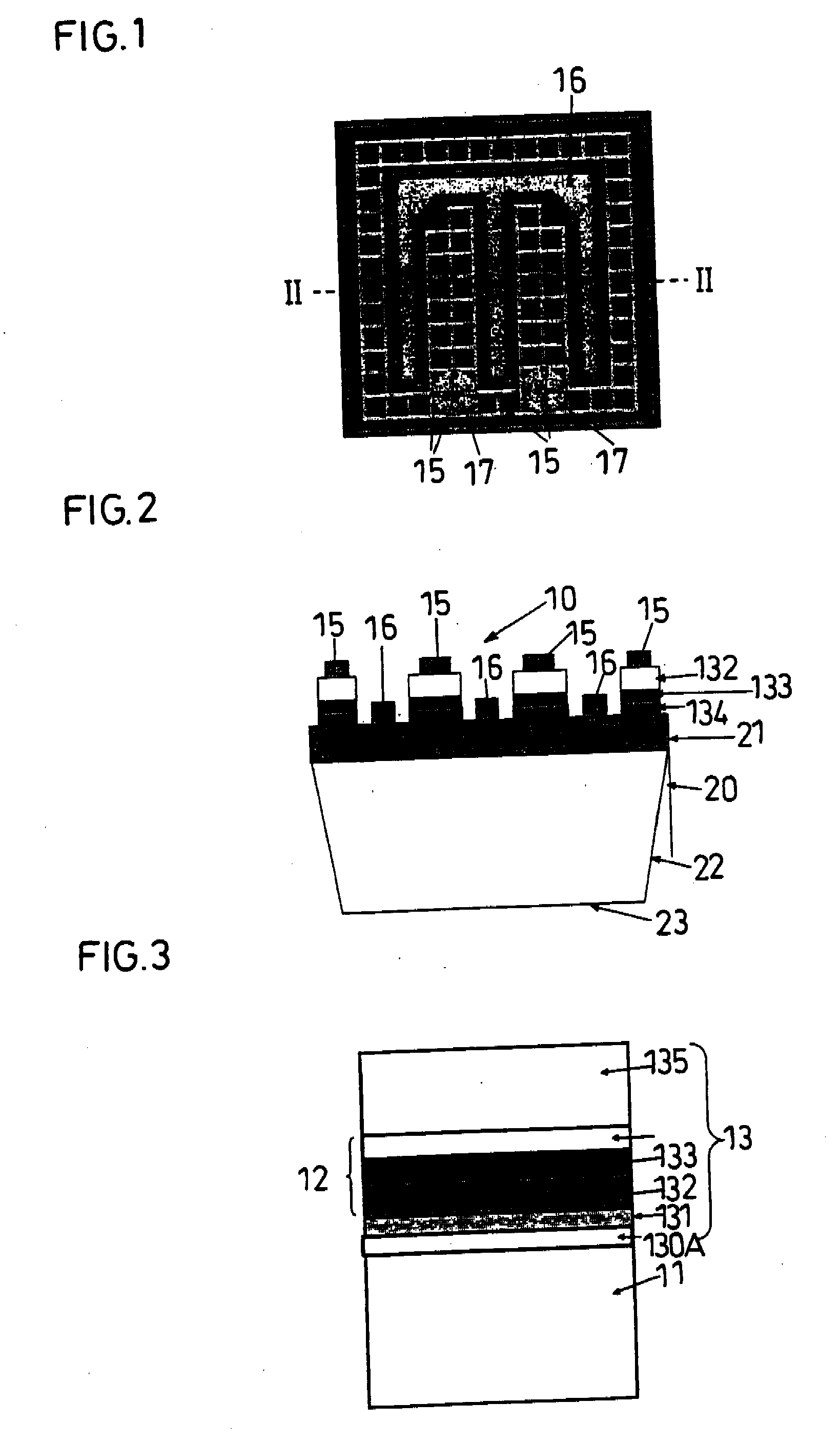
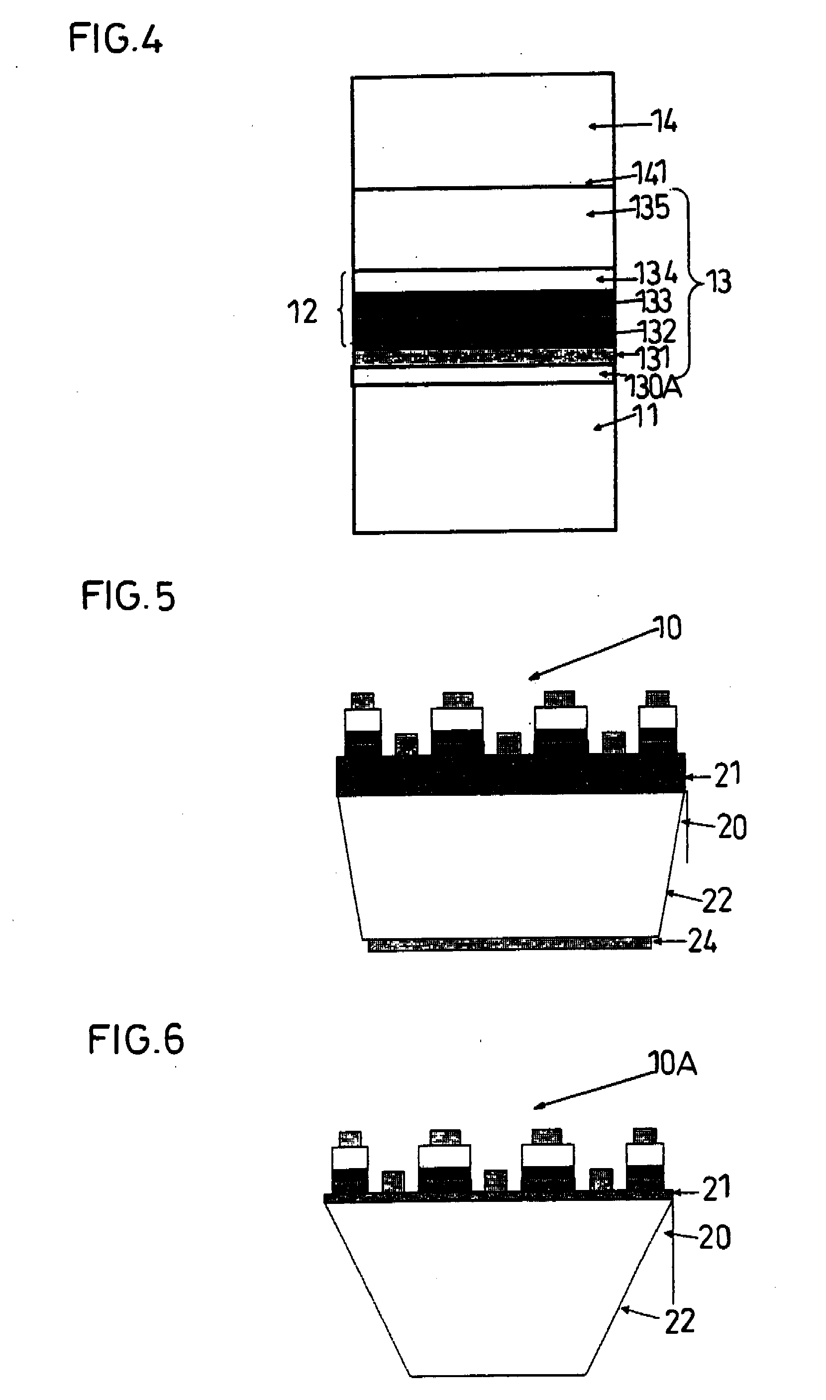
[0124]FIG. 1 and FIG. 2 schematically illustrate a semiconductor light-emitting diode 10 fabricated in Example 1. FIG. 1 is a plan view and FIG. 2 is a cross section taken across FIG. 1 along line II-II. FIG. 3 is a schematic cross section of the layered structure of a semiconductor epitaxial stacked structure to be used in the semiconductor light-emitting diode 10 of Example 1 and FIG. 4 is a schematic cross section illustrating a structure resulting from joining a substrate 14 to the semiconductor epitaxial stacked structure of FIG. 3.

[0125]The semiconductor light-emitting diode 10 fabricated in Example 1 was a red color Light-Emitting Diode (LED) possessing an AlGaInP light-emitting part 12. It was fabricated by joining an epitaxial stacked structure formed on a semiconductor substrate 11 made of GaAs and the GaP substrate 14.

[0126]The light-emitting diode 10 was fabricated by using an epitaxial wafer that was furnished with an epitaxial growth layer 13 composed of semiconductor ...

example 2

[0141]A semiconductor light-emitting diode 10 of Example 2 possessing the same structure as in Example 1 while having a metal layer 24 of an AuSn eutectic (melting point 283° C.) formed on the back surface as illustrated in FIG. 5 was fabricated.

[0142]A semiconductor Light-Emitting Diode lamp (LED lamp) 1 possessing the structure illustrated schematically in FIG. 8 and FIG. 9 was assembled by following the same procedure as in the use of the semiconductor light-emitting diode 10 of Example 1 while using the semiconductor light-emitting diode 10 of Example 2 as an LED chip 42 and using AuSn in the place of the Ag paste.

[0143]The semiconductor light-emitting diode lamp1 that was manufactured by using the semiconductor light-emitting diode 10 of Example 2 was evaluated in the same manner as in Example 1. The results are shown in Table 1 below. The forward voltage (Vf) during the flow of an electric current of 500 mA in the forward direction was 2.4 V. The intensity of light emission wa...

example 3

[0148]As another concrete example of the second embodiment, the light-emitting diode according to Example 3 will be described below by reference to the accompanying drawings.

[0149]FIG. 10 and FIG. 11 illustrate the semiconductor light-emitting diode 10 of Example 3; FIG. 10 is a plan view and FIG. 11 is a cross section taken across FIG. 10 along line XI-XI. FIG. 12 is a schematic cross section of the layered structure of the semiconductor epitaxial stacked structure used in the light-emitting diode 10 of Example 3 and FIG. 13 is a schematic cross section illustrating a structure resulting from joining the GaP substrate 14 to the semiconductor epitaxial stacked structure of FIG. 12.

[0150]The semiconductor light-emitting diode 10 of Example 3 was a red color Light-Emitting Diode (LED) possessing an AlGaInP light-emitting part 12 and was fabricated by joining an epitaxial stacked structure installed on a semiconductor substrate 11 made of GaAs to the GaP substrate 14.

[0151]The light-em...


PUM


Abstract

A transparent-substrate light-emitting diode (10) has a light-emitting layer (133) made of a compound semiconductor, wherein the area (A) of a light-extracting surface having formed thereon a first electrode (15) and a second electrode (16) differing in polarity from the first electrode (15), the area (B) of a light-emitting layer (133) formed as approximating to the light-extracting surface and the area (C) of the back surface of a light-emitting diode falling on the side opposite the side for forming the first electrode (15) and the second electrode (16) are so related as to satisfy the relation of A>C>B. The light-emitting diode (10) of this invention, owing to the relation of the area of the light-emitting layer (133) and the area of the back surface (23) of the transparent substrate and the optimization of the shape of a side face of the transparent substrate (14), exhibits high brightness and high exoergic property never attained heretofore and fits use with an electric current of high degree.

Description

CROSS REFERENCE TO RELATED APPLICATIONS[0001]This application is an application filed under 35 U.S.C. §111(a) claiming the benefit pursuant to 35 U.S.C. §119(e)(1) of the filing dates of Provisional Applications No. 60 / 754,894 filed Dec. 30, 2005, No. 60 / 754,895 filed Dec. 30, 2005 and No. 60 / 754,320 filed Dec. 29, 2005 and Japanese Patent Applications No. 2005-369334 filed Dec. 22, 2005, No. 2005-369620 filed Dec. 22, 2005, and No. 2005-369996 filed Dec. 22, 2005 pursuant to 35 U.S.C. §111(b).TECHNICAL FIELD[0002]This invention relates to a transparent-substrate light-emitting diode provided with a light-emitting layer made of a compound semiconductor, and furnished with a light-extracting surface having formed thereon a first electrode and a second electrode possessing polarity different from the first electrode. More particularly, this invention relates to a light-emitting diode excelling in exoergic property and exhibiting high brightness and to a method for the fabrication ther...

Claims


Application Information

Patent Timeline
Patent Type & Authority Applications(United States)
IPC IPC(8): H01L33/00H01L21/28H01L33/20H01L33/38
CPCH01L33/38H01L33/20H01L2224/45144H01L2224/48091H01L2224/48465H01L2224/49107H01L2924/00014H01L2924/00
Inventor NABEKURA, WATARUTAKEUCHI, RYOUICHI
Owner SHOWA DENKO KK
Why Eureka
Try Eureka