Semiconductor device

a semiconductor and reverse-coating technology, applied in semiconductor devices, diodes, electrical devices, etc., can solve the problems of adversely affecting the conductivity modulation phenomenon, increasing voltage, and difficulty in forming an optimal structure for both elements in the same semiconductor substrate, so as to reduce the recovery current, shorten the life of the hole, and reduce the recovery loss

Inactive Publication Date: 2009-11-12
TOYOTA JIDOSHA KK
View PDF1 Cites 62 Cited by
  • Summary
  • Abstract
  • Description
  • Claims
  • Application Information

AI Technical Summary

Benefits of technology

[0010]The present invention provides a reverse conducting semiconductor device in which both an IGBT element region and a diode element region are provided in the same semiconductor substrate, and that reduces the recovery loss in the diode element region without increasing the ON-state voltage in the IGBT element region.
[0011]An aspect of the present invention relates to a reverse conducting semiconductor device in which both an IGBT element region and a diode element region are formed on the same semiconductor substrate. This semiconductor device includes: a p-type collector layer, an n-type drift layer, and a p-type body layer that are laminated in order in the IGBT element region; a trench gate electrode that extends through the body layer from a front surface of the body layer to project into the drift layer; an insulating film that surrounds the trench gate electrode; an n-type emitter region that is in contact with the insulating film and is formed in an area facing the front surface of the body layer, in which the emitter region is separated from the drift layer by the body layer; an n-type cathode layer, the drift layer, and a p-type anode layer that are laminated in order in the diode element region; an anode region that is formed in an area that faces a front surface of the anode layer, and contains a p-type impurity at higher concentration than in the anode layer, in which the anode region is separated from the drift layer by the anode layer; and a low lifetime region that is formed in at least a part of the drift layer within the diode element region, and shortens a lifetime of a hole. A mean value of a lifetime of a hole in the drift layer that includes the low lifetime region is shorter within the diode element region than within the IGBT element region.
[0012]According to the above-mentioned semiconductor device, the low lifetime region is provided in at least a part of the drift layer within the diode element region. Thus, at the time of a recovery operation in which the diode element region is shifted from a conductive state to a non-conductive state, some of the holes that return to the anode layer are lost in the low lifetime region. This makes it possible to reduce recovery current in the diode element region, thus enabling reduction in recovery loss in the diode element region. Also, in the above-mentioned semiconductor device, the mean value of the lifetime of a hole in the drift layer that includes the low lifetime region is shorter within the IGBT element region than within the diode element region. In the IGBT element region, the holes that exist in the drift layer when the IGBT element region is in the ON state are not easily lost, and conductivity modulation is actively performed. Thus, the ON-state voltage in the IGBT element region does not increase. According to the above-mentioned semiconductor device, recovery loss in the diode element region can be reduced without increasing the ON-state voltage in the IGBT element region.
[0013]According to the present invention, recovery loss in the diode element region can be reduced without increasing the ON-state voltage in the IGBT element region.

Problems solved by technology

Because two kinds of elements exist in reverse conducting semiconductor devices, it is difficult to form an optimal structure for both of the elements in the same semiconductor substrate.
However, in the IGBT element region J101, this is likely to adversely affect the conductivity modulation phenomenon when the low lifetime layer 161 is in an ON state, thereby increasing the voltage in the IGBT element region J101.

Method used


Image

  • Semiconductor device
  • Semiconductor device
  • Semiconductor device

Examples


Embodiment Construction

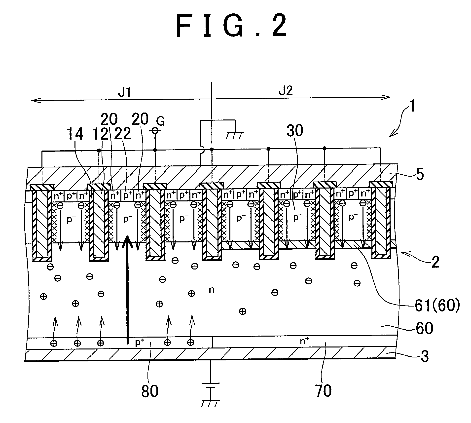
[0029]The main features of a semiconductor device according to an embodiment of the present invention, which will be described in the following, are listed below. A low lifetime region of the semiconductor device is formed at least within a drift layer near the boundary between an anode layer and the drift layer. After a resist is formed on an area of the front surface of a semiconductor layer that is to become an IGBT element region of the semiconductor device, a non-conductive impurity is implanted from the front surface side. The acceleration voltage at the time when the non-conductive impurity is implanted from the front surface side is set in such a way that the peak of the concentration of the non-conductive impurity to be implanted occurs within the drift layer near the boundary between the anode layer and the drift layer.

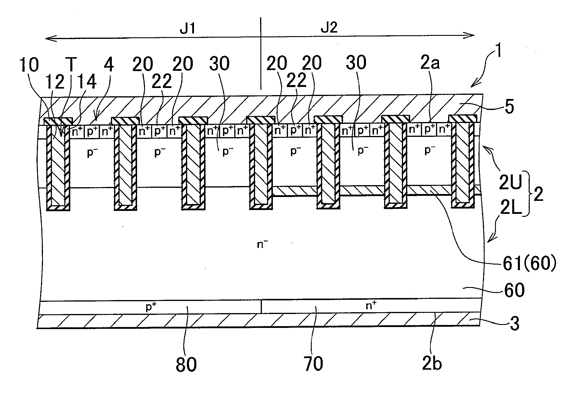
[0030]FIG. 1 is a sectional view of the main portion of a reverse conducting semiconductor device 1 in which an IGBT element region J1 and a diode element r...


PUM


Abstract

A semiconductor device in which both an IGBT element region and a diode element region exist in the same semiconductor substrate includes a low lifetime region, which is formed in at least a part of a drift layer within the diode element region and shortens the lifetime of holes. A mean value of the lifetime of holes in the drift layer that includes the low lifetime region is shorter within the IGBT element region than within the diode element region.

Description

INCORPORATION BY REFERENCE[0001]The disclosure of Japanese Patent Application No. 2008-123618 filed on May 9, 2008 including the specification, drawings and abstract is incorporated herein by reference in its entirety.BACKGROUND OF THE INVENTION[0002]1. Field of the Invention[0003]The present invention relates to a reverse conducting semiconductor device in which both an insulated gate bipolar transistor (IGBT) element region and a diode element region are provided in the same semiconductor substrate.[0004]2. Description of the Related Art[0005]Reverse conducting semiconductor devices exist in which both a region where an insulated gate bipolar transistor (IGBT) is formed (IGBT element region) and a region where an free wheel diode (FWD) is formed (diode element region) exist in the same semiconductor substrate. Because two kinds of elements exist in reverse conducting semiconductor devices, it is difficult to form an optimal structure for both of the elements in the same semiconduc...

Claims


Application Information

Patent Timeline
Patent Type & Authority Applications(United States)
IPC IPC(8): H01L29/739
CPCH01L27/0664H01L29/861H01L29/7397
Inventor SOENO, AKITAKAHISANAGA, YUKIHIRO
Owner TOYOTA JIDOSHA KK
Why Eureka
Try Eureka