Laminated Ceramic Electronic Component and Method for Producing the Same

Active Publication Date: 2009-11-12
MURATA MFG CO LTD
View PDF16 Cites 23 Cited by
  • Summary
  • Abstract
  • Description
  • Claims
  • Application Information

AI Technical Summary

Benefits of technology

[0010]In addition, preferred embodiments of the present invention provide a method for producing a laminated ceramic electronic component in which a decrease in the permeability due to the magnetostrictive effect is prevented.
[0012]According to the structure described above, the thickness of the lead conductor is small. Therefore, although mechanical stress during cutting is directly applied to the lead conductor, the mechanical stress applied to the lead conductor during cutting is reduced.
[0017]A small thickness of the lead conductor decreases the cross-sectional area of the lead conductor so as to increase the direct current resistance. Accordingly, the conductor width of the lead conductor is preferably greater than the conductor width of the inner conductor. Thus, the decrease in the cross-sectional area of the lead conductor is compensated for. As a result, the increase in the direct current resistance caused by decreasing the thickness of the lead conductor is prevented.
[0019]Among the inner conductor pattern layers, at least the inner conductor pattern layer that is in contact with the ceramic green sheet is preferably formed with conductive paste including resin particles that are consumed during the firing process. When the resin particles are consumed during the firing process, a space is formed between the ceramic green sheet and the inner conductor. As a result, the stress applied to the ceramic green sheet (ferrite) is reduced to prevent the decrease in the permeability caused by the magnetostrictive effect. Furthermore, the formation of this space prevents cracks from generating on the inner conductor.
[0020]As described above, according to preferred embodiments of the present invention, the thickness of a lead conductor is less than that of an inner conductor. Accordingly, the mechanical stress applied to the lead conductor during cutting is reduced. As a result, defects, such as cracking generated on the lead conductor during cutting, are prevented.
[0021]In addition, among inner conductor pattern layers, at least an inner conductor pattern layer that is in contact with ceramic green sheets is formed with conductive paste including resin particles that are consumed during the firing process. Accordingly, the decrease in the permeability caused by the magnetostrictive effect is prevented.

Problems solved by technology

Therefore, defects such as cracking are typically not generated.
However, with such a large thickness of the conductor, when the mother ceramic laminated block is cut, excessive mechanical stress is applied to the lead portion of the conductor for a coil.
As a result, defects such as cracking are often generated.

Method used


Image

  • Laminated Ceramic Electronic Component and Method for Producing the Same
  • Laminated Ceramic Electronic Component and Method for Producing the Same
  • Laminated Ceramic Electronic Component and Method for Producing the Same

Examples


Embodiment Construction

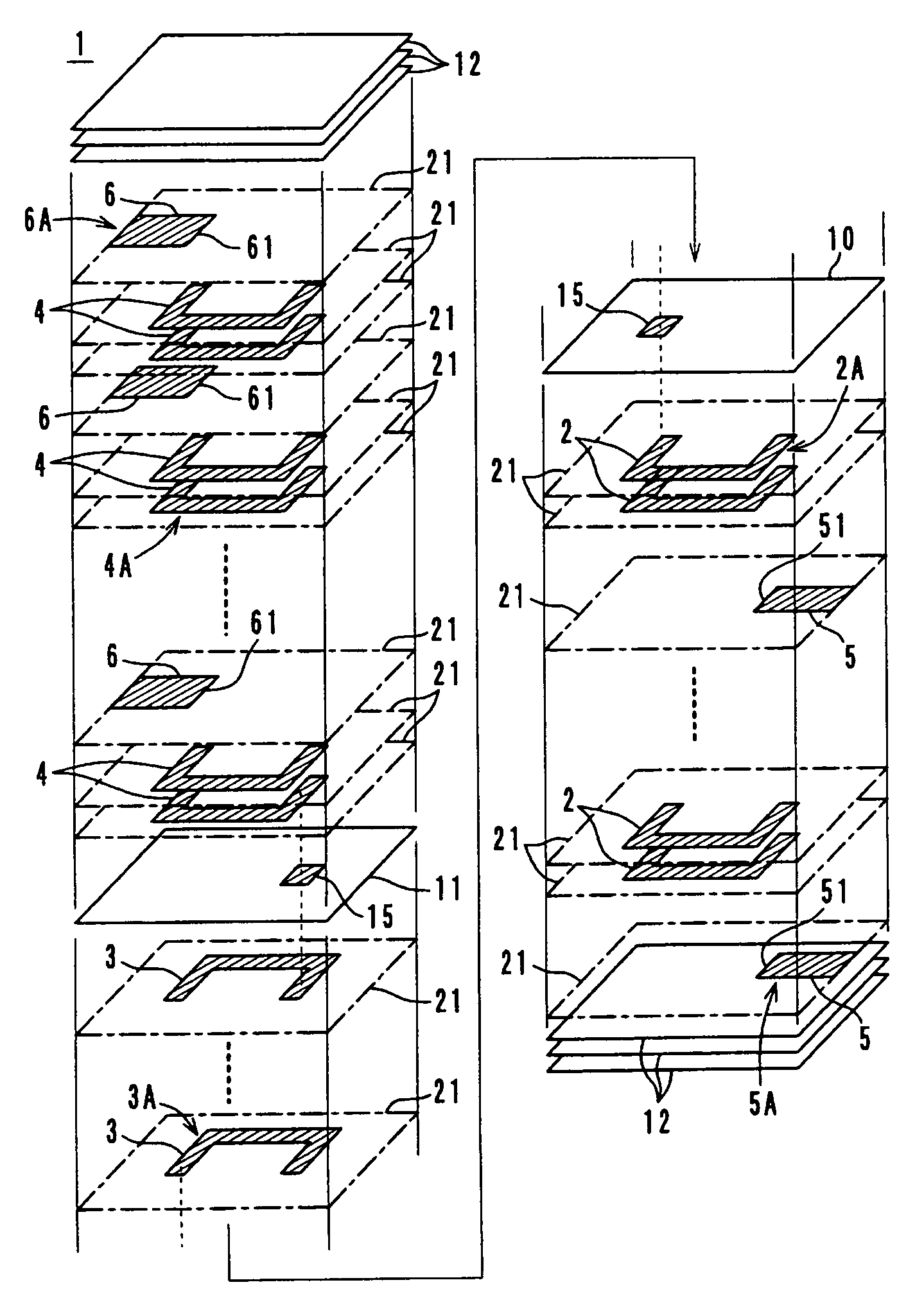
[0040]Preferred embodiments of a laminated ceramic electronic component according to the present invention and a method for producing the same will now be described with reference to the attached drawings.

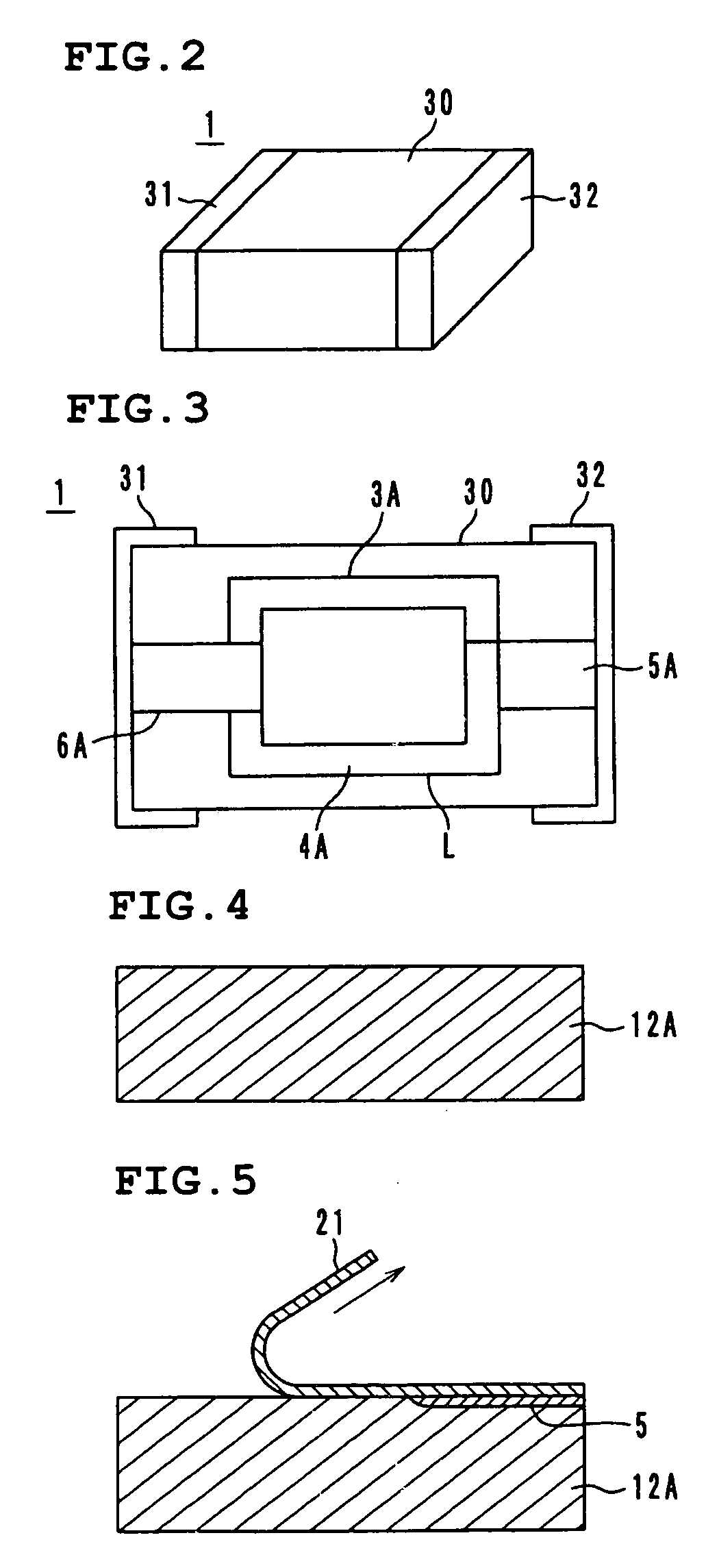
[0041]As shown in FIG. 1, a laminated inductor 1 includes, for example, conductor pattern layers 2, 3, and 4 for a coil, lead conductor pattern layers 5 and 6, and ceramic green sheets 10, 11, and 12. Reference numeral 21 indicates a support (carrier film). As will be described below, the support (carrier film) 21 is eventually removed and is not included in the laminated inductor 1.

[0042]The ceramic green sheets 10 to 12 are formed as follows. For example, a Fe—Ni—Cu-containing ferrite powder or a glass ceramic powder is mixed with a binder. The mixture is formed by, for example, a doctor blade method so as to have a sheet shape. The ceramic green sheets 12 are used for outer layers, whereas the ceramic green sheets 10 and 11 are used as inner layers.

[0043]Via holes 15 for inner l...


PUM

PropertyMeasurementUnit
Thicknessaaaaaaaaaa
Thicknessaaaaaaaaaa
Thicknessaaaaaaaaaa

Abstract

A laminated ceramic electronic component includes a plurality of conductor pattern layers for a coil arranged to overlap each other to form substantially U-shaped conductors for the coil. The conductors for the coil are electrically connected in series through via holes for inner layer connection provided in ceramic green sheets to form a spiral coil. A plurality of lead conductor pattern layers also overlaps each other to form lead conductors. One lead conductor pattern layer is disposed per a predetermined number of conductor pattern layers for the coil. An end of each lead conductor pattern layer is in contact with the corresponding conductor pattern layer for the coil. In other words, the thickness of the lead conductors is less than the thickness of the conductors for the coil.

Description

BACKGROUND OF THE INVENTION[0001]1. Field of the Invention[0002]The present invention relates to a laminated ceramic electronic component, and in particular, to a laminated ceramic electronic component such as a laminated inductor, a laminated impedance component, a laminated transformer, and a high frequency line device, and a method for producing the same.[0003]2. Description of the Related Art[0004]In general, a laminated ceramic electronic component such as a laminated inductor is produced as follows. Firstly, a mother ceramic laminated block including a plurality of ceramic laminated products is formed. The mother ceramic laminated block is cut according to the arrangement of inner conductors, such as conductors for a coil and lead conductors, to provide each ceramic laminated product. The resultant ceramic laminated product is fired. Subsequently, outer electrodes are formed on the surface of the ceramic laminated product to provide a final product.[0005]When the inner conduct...

Claims


Application Information

Patent Timeline
IPC IPC(8): H01F5/00B32B37/00H01F17/00H01F27/29
CPCH01F17/0013H01F27/292H01F2017/0093H05K3/246H01F41/042Y10T29/49078H01F41/0233H01F41/34Y10T29/49075Y10T29/4902H01F41/043H01F17/00H01F27/29
Inventor TATSUKAWA, TSUYOSHITAKAYAMA, KEISUKE
Owner MURATA MFG CO LTD
Why Eureka
Try Eureka