Etching method and etching apparatus of semiconductor wafer

a technology of etching apparatus and semiconductor wafer, which is applied in the direction of semiconductor/solid-state device testing/measurement, fluid pressure measurement, instruments, etc., can solve the problems of difficult surface monitoring, difficult to monitor the depth of etching during the actual etching, and practicably inability to realize feedback in the middle of polishing

Active Publication Date: 2009-11-19
SUMCO TECHXIV
View PDF6 Cites 26 Cited by
  • Summary
  • Abstract
  • Description
  • Claims
  • Application Information

AI Technical Summary

Problems solved by technology

However, it is difficult to monitor how deep the wafer is etched during the actual etching in a so-called wet state using a hydrogen fluoride solution to which an oxidant such as nitric acid or hydrogen peroxide is added.
It is likewise difficult to monitor the surface being polished by a chemical polishing method or the like, thereby being practically unable to realize feedback in the middle of polishing.
Here, even if it is etching with a mixture gas of hydrogen fluoride gas and water vapor, which is further mixed with ozone, the silicon wafer surface would get wet such that the etching is substantially conducted in a wet condition and, thus, it is

Method used


Image

  • Etching method and etching apparatus of semiconductor wafer
  • Etching method and etching apparatus of semiconductor wafer
  • Etching method and etching apparatus of semiconductor wafer

Examples


Embodiment Construction

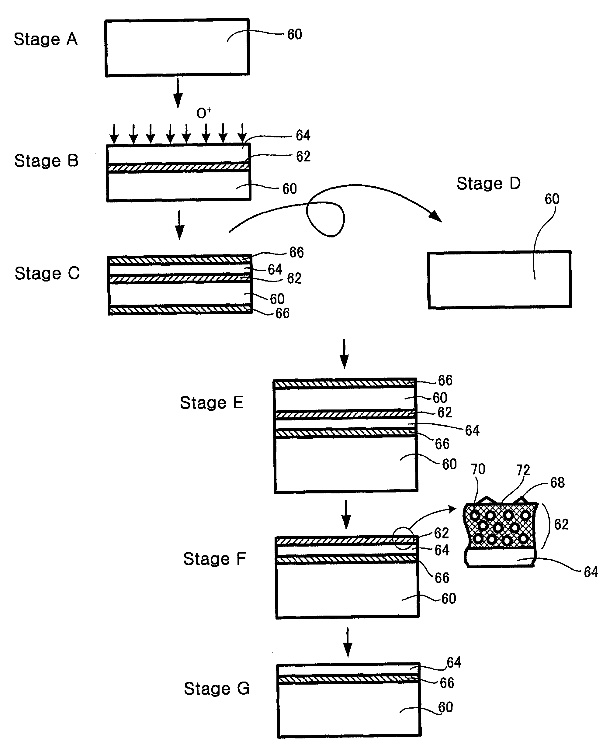
[0019]Now, embodiments of the present invention are described below with reference to the attached drawings and the following description is provided for describing the embodiments of the present invention and the present invention is not limited to the embodiments. The same or related symbols refer to the same or the same type of elements and redundant description may be omitted.

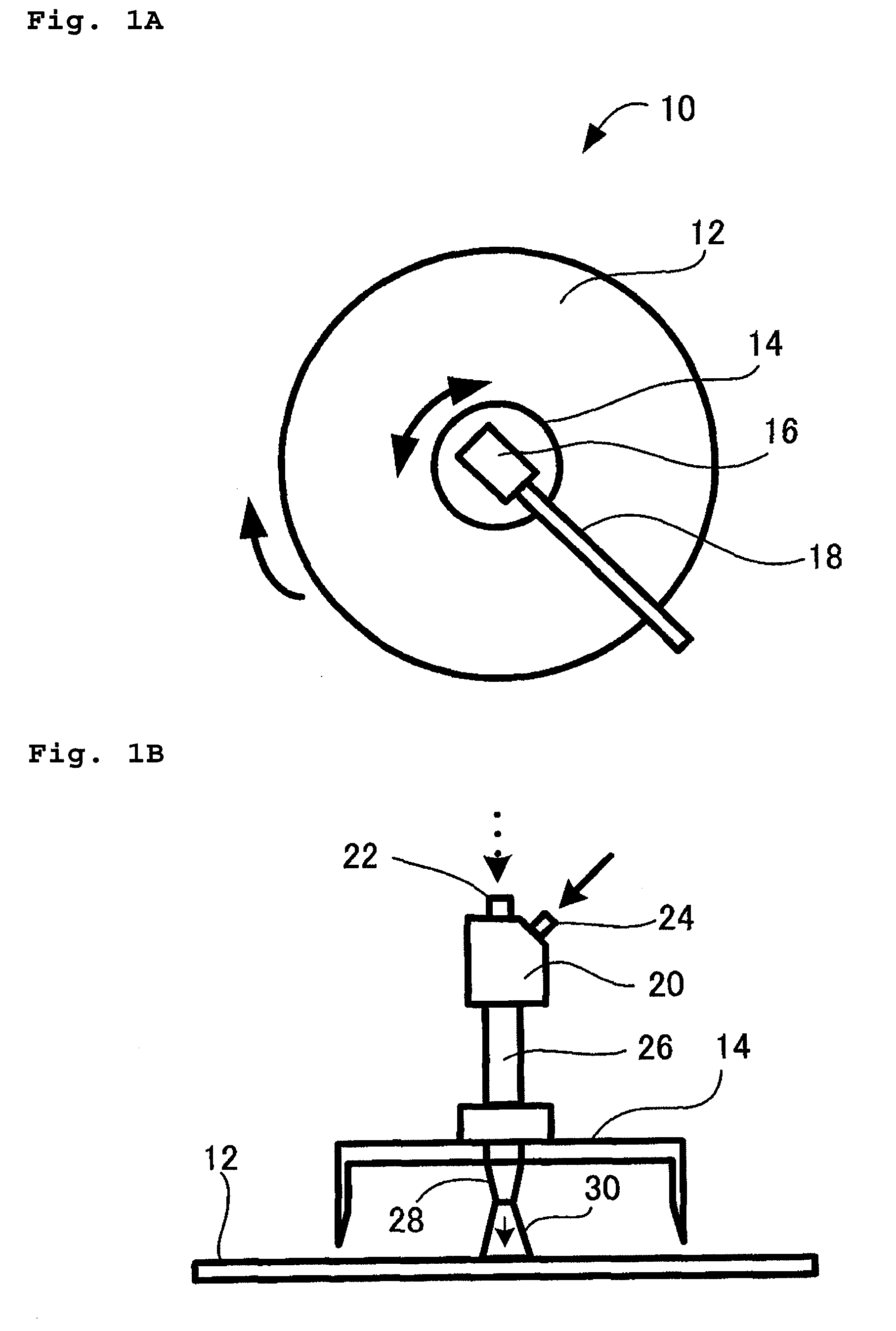
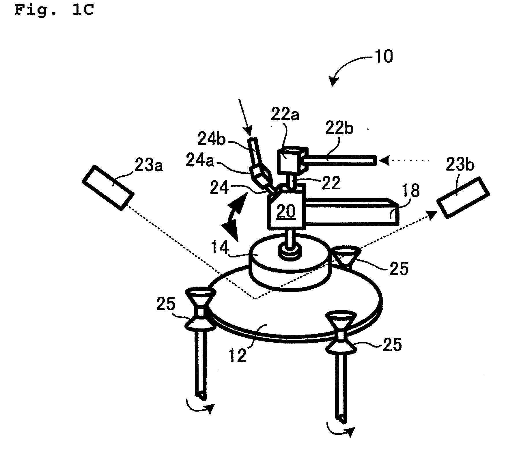
[0020]FIG. 1A is a plan view showing a general configuration of an etching apparatus 10 according to an embodiment of the present invention and FIG. 1B is a sectional view thereof. A silicon wafer 12 is set in the apparatus 10 rotatably in a clockwise manner as indicated by the arrow and a cone 14 is suspended thereabove from a mixer 16 in which a mixed gas for etching is prepared. The mixer 16 is fixed to a swinging arm 18 that swings as indicated by the arrows. This configuration is now described in more detail in reference to the schematic sectional view. The mixer 16 includes a mixing container 20, port...


PUM

PropertyMeasurementUnit
Concentrationaaaaaaaaaa

Abstract

A method of etching a semiconductor wafer is provided. The method comprises the steps of: jetting a mixed gas including hydrogen fluoride and ozone onto a surface of a semiconductor wafer; monitoring the surface of the semiconductor wafer; analyzing the surface of the semiconductor wafer; and adjusting at least one of the hydrogen fluoride concentration and the ozone concentration in the mixed gas based on a result of the analysis.

Description

CROSS REFERENCE TO RELATED APPLICATIONS[0001]This application claims priority to Japanese Patent Application No. 2008-128944 filed on May 15, 2008, the entire contents of which are incorporated herein by reference.FIELD OF THE INVENTION[0002]The present invention relates to an etching method and an etching apparatus of a semiconductor wafer. More specifically, the present invention relates to an etching method and an etching apparatus using a mixed gas that contains hydrogen fluoride and ozone.BACKGROUND ART[0003]In etching of the semiconductor wafer such as silicon wafer, both wet and dry processes may apply. In the wet type, a method of immersing the wafer in a mixed acid of HF / HNO3 or in an alkali solution of NaOH, KOH, or the like is generally utilized. A method of processing the wafer with the mixed acid is also partially used in a single-wafer spinning manner. Further, in the dry type, an etching method of irradiating the wafer with excited ions or radicals generated by plasma...

Claims


Application Information

Patent Timeline
IPC IPC(8): H01L21/66H01L21/306
CPCH01L21/31116H01L21/76243H01L22/26H01L22/12H01L21/76256
Inventor KOZASA, KAZUAKIKAWASAKI, TOMONORI
Owner SUMCO TECHXIV
Why Eureka
Try Eureka