Electro-optical device, matrix substrate, and electronic equipment

a technology of electrooptical devices and matrix substrates, applied in static indicating devices, identification means, instruments, etc., can solve the problems of exponential display increase, uneven display, and lowered display performance, so as to reduce or prevent an increase in electrical power consumption and reduce display performance

Inactive Publication Date: 2009-11-26
SEIKO EPSON CORP
View PDF22 Cites 11 Cited by
  • Summary
  • Abstract
  • Description
  • Claims
  • Application Information

AI Technical Summary

Benefits of technology

[0006]When using electrically driven light-emitting elements, such as organic EL elements for large displays, it is advantageous to reduce or prevent an increase in electrical power consumption due to the resistance of

Problems solved by technology

When the distribution of the electrical current supplied to the entire screen is not uniform, the display becomes uneven and the display performance is lowered.
As the display becomes large, the number of pixels needed for the display increas

Method used


Image

  • Electro-optical device, matrix substrate, and electronic equipment
  • Electro-optical device, matrix substrate, and electronic equipment
  • Electro-optical device, matrix substrate, and electronic equipment

Examples


exemplary embodiment 1

[0050]This exemplary embodiment is described below by referring to the drawings.

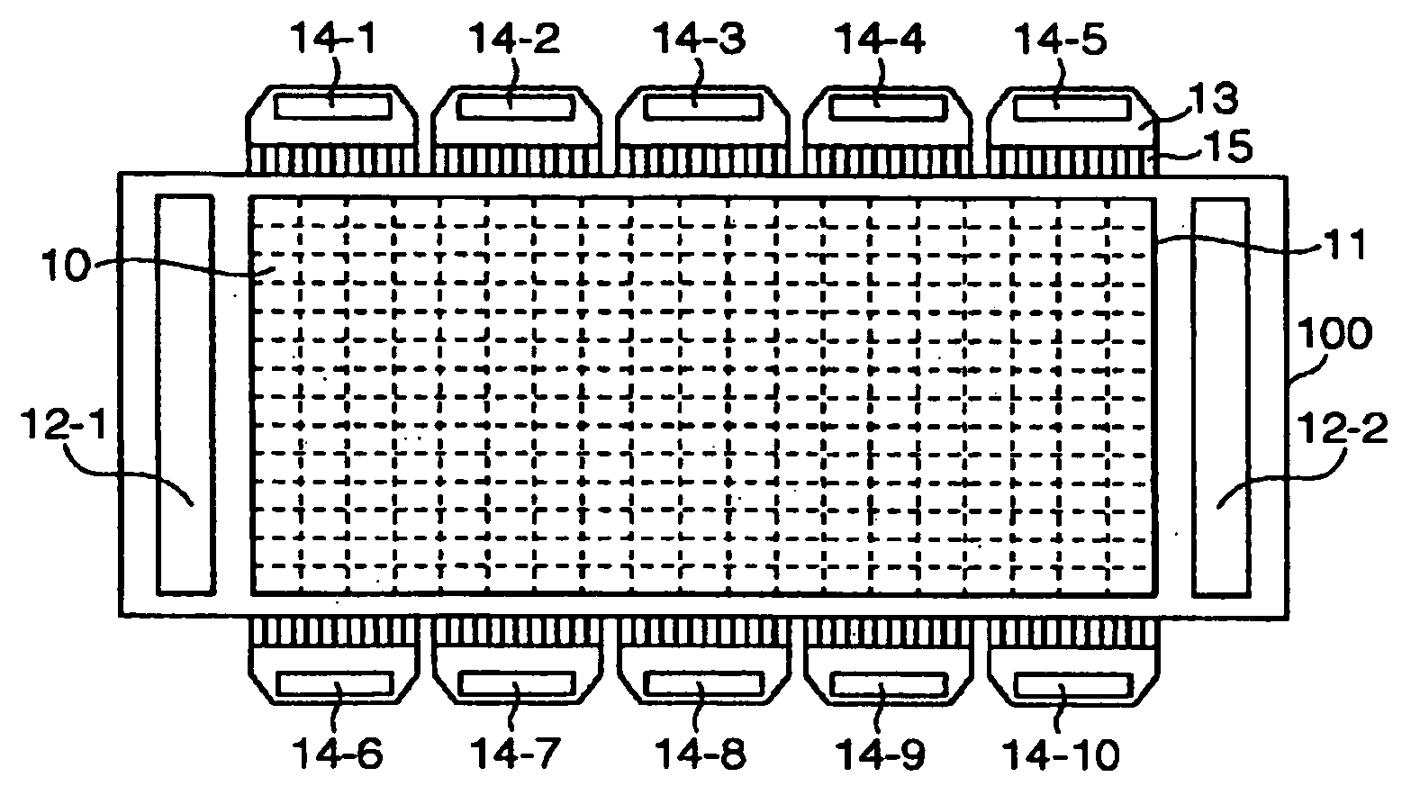
[0051]FIG. 1 is a schematic of an overview of an organic EL display panel. The panel includes a plurality of pixels 10 arranged in a matrix with N rows and M columns. The panel has a pixel area 11 that forms a pixel matrix, an active matrix substrate 100 including scanning line drivers 12-1 and 12-2 that output scanning line signals to each pixel 10, and ten driver IC chips 14-1 to 14-10 lead-bonded to the outside edges of the active matrix substrate 100. The driver IC chips 14-1 to 14-10 each include a data line driver that sends data signals to each pixel 10. The driver IC chips 14-1, 14-5, 14-6, and 14-10, which are each located on the corners of the active matrix substrate 100, have power-supply circuits for supplying power to the active matrix substrate 100. The driver IC chips 14-1 to 14-10 are disposed by tape automated bonding (TAB) enclosed on tape carrier packages 13 with output leads 15 connec...

exemplary embodiment 2

[0059]FIG. 4 is a schematic of the arrangement of power-supply wiring related to a second exemplary embodiment according to the present invention. FIG. 6 is a schematic showing the main circuit of a pixel 10 located in row n, column m according to this exemplary embodiment. Within the drawing, reference numerals that are the same as FIGS. 3 and 5 represent the same elements as those of FIGS. 3 and 5 and the descriptions are omitted. In FIG. 6, taking a close look at a red pixel 10, this pixel 10 includes a switching transistor Tr1, whose gate terminal connects to a scanning line 17-(3n−2), a capacitor C, which maintains a data signal sent from a data line Xm for one frame period, a light emitting portion OLED composed of an organic EL element, and a driving transistor Tr2, which receives power from a main power line VR and supplies driving power to a light-emitting portion OLED. Green and blue pixels 10 also have the same circuit structure, receive power from main power-supply lines...

exemplary embodiment 3

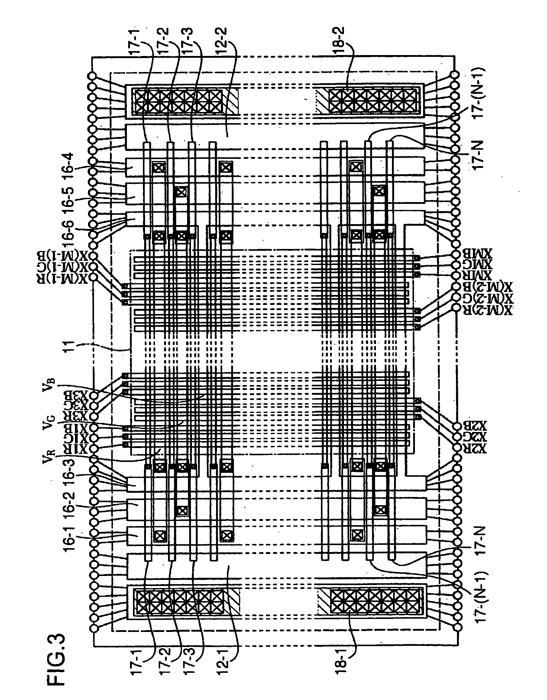
[0060]FIG. 7 is a schematic of the arrangement of power-supply wiring related to a third exemplary embodiment. In the drawing, only the power-supply wiring is shown and data lines, scanning lines, and cathode contacting portion are not shown to simplify the description. This exemplary embodiment is similar to exemplary embodiment 1 in that basic power-supply lines 16-1 to 16-3 are arranged in the vicinity of the outside edge of pixel area 11 shown on the left side of the drawing and basic power-supply lines 16-4 to 16-6 are arranged in the vicinity of the outside edge of the pixel area 11 shown on the right side of the drawing. The basic power-supply lines 16-1 and 16-4 are power-supply lines to supply an anode power supply to red organic EL elements and are connected to main power-supply lines VR arranged on the pixel area 11 in the row direction in a strip pattern. Similarly, the basic power-supply lines 16-2 and 16-5 are power-supply lines to supply an anode power to green organi...


PUM


Abstract

The invention provides power-supply wiring preferable for large displays. An electro-optical device according to the present invention includes a pixel area including electro-optical elements driven by power supplied from power-supply circuits. The electro-optical device includes basic power-supply lines, which receive a power-supply voltage output from the power-supply circuits and which are formed on the upper portion of a substrate, and includes main power-supply lines which intersect the basic power-supply lines and which are formed on the upper portion of the substrate. The power-supply voltage is supplied to the electro-optical elements via the main power-supply lines.

Description

[0001]This is a Continuation of application Ser. No. 10 / 636,569 filed Aug. 8, 2003, which claims priority to Japanese Applications Nos. 2002-272063 and 2003-286295 filed Sep. 18, 2002 and Aug. 4, 2003. The disclosures of the prior applications are hereby incorporated by reference herein in their entirety.BACKGROUND OF THE INVENTION[0002]1. Field of Invention[0003]The present invention relates to an arrangement of power-supply wiring of an electro-optical device suitable for a large display panel.[0004]2. Description of Related Art[0005]Since organic EL elements are electrically driven light-emitting elements, a backlight is not needed. Additional advantages include their low electrical power consumption, wide field of view, and high contrast ratio. Organic EL elements are used for small and medium size displays for devices, such as cellular phones and personal digital assistants. An organic EL element is an electro-optical element with a light-emitting layer including fluorescent ma...

Claims


Application Information

Patent Timeline
IPC IPC(8): G09G5/00G09F9/00G09F9/30H05B33/06G09G3/20G09G3/30G09G3/32H01L27/00H01L27/32H01L51/50H05B33/14H05B33/26
CPCG09G3/3233G09G2300/0426G09G2300/0842H01L27/3276G09G2310/0297H01L27/3211G09G2310/0221H10K59/35H10K59/131H05B33/26
Inventor MATSUEDA, YOJIRONAKANISHI, HAYATO
Owner SEIKO EPSON CORP
Why Eureka
Try Eureka