Light emitting device with a non-activated luminescent material

a luminescent material and light-emitting device technology, applied in the direction of luminescent compositions, semiconductor devices, chemistry apparatus and processes, etc., can solve the problems of high requirements for diffusing particles, insufficient effect to remove directional dependence of blue light, and non-uniform emission characteristics, so as to achieve a strong scattering effect and increase the number of scattering events

Inactive Publication Date: 2009-12-03
TRIDONIC OPTOELECTRONICS GMBH
View PDF10 Cites 14 Cited by
  • Summary
  • Abstract
  • Description
  • Claims
  • Application Information

AI Technical Summary

Benefits of technology

[0034]Advantageously the diffusing particles have a diameter between about 1 and about 40 μm. The number of diffusing particles can thereby advantageously be selected in dependence upon the (average) diffusing particle size. The smaller the (averag

Problems solved by technology

Additionally to this, an LED is typically substantially cube-shaped which itself, that is solely due to the geometric conditions, already brings about a non-uniform emission characteristic.
The blue light is also scattered to a certain extent at the luminescent material particles but as a rule this effect does not suffice to remove the directional dependence of the blue light.
With the mentioned stat

Method used


Image

  • Light emitting device with a non-activated luminescent material
  • Light emitting device with a non-activated luminescent material
  • Light emitting device with a non-activated luminescent material

Examples


Embodiment Construction

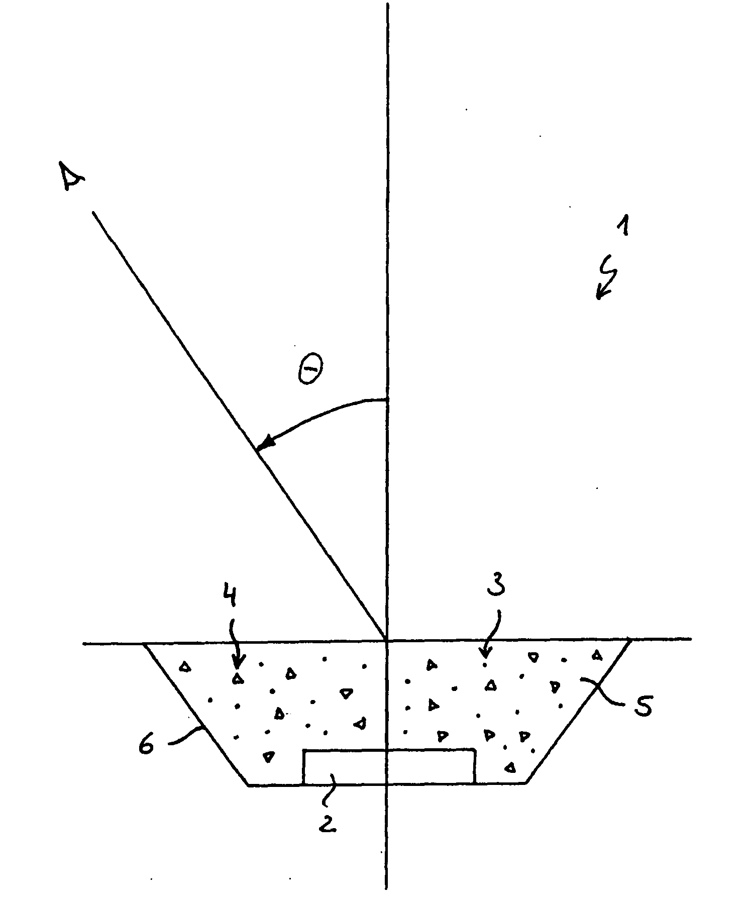
[0056]FIG. 1 shows a light emitting device 1. The device has as radiation emitting element, including a semiconductor, a light-emitting diode (LED) 2. The LED 2 radiates for example blue light, upwardly with reference to the illustration. With regard to the electrical components which are necessary for the activation of the LED nothing is said here since they are without immediate relevance for the invention. In this regard attention is directed to the state of the art.

[0057]Furthermore the device 1 has a luminescent material in the form of fluorescent particles 3. The fluorescent particles 3, also called luminescent material particles, are able to absorb a part of the radiation which is sent out by the LED 2 and to send out light with a wavelength which is different from the wavelength of the absorbed radiation. The radiation sent out by the luminescent material particles 3 can for example be yellow light. In the case of the radiation which is sent out by the LED 2 and is absorbed ...


PUM


Abstract

The invention relates to a light emitting device having a radiation emitting element, for example a light emitting diode, and a luminescent material which is able to absorb a part of the radiation sent out by the radiation emitting element and to send out light with a wavelength which is different from the wavelength of the absorbed radiation. The device further has diffusing particles which are able to scatter a part of the radiation sent out by the radiation emitting element, and/or to scatter a part of the light sent out by the luminescent material. The diffusing particles are of non-activated luminescent material, through which production is simplified.

Description

TECHNICAL FIELD OF THE INVENTION[0001]The invention relates to a light emitting device with a radiation emitting element which includes a semiconductor. The device has a luminescent material which is able to absorb a part of the radiation sent out by the radiation emitting element and send out light with a wavelength which is different from the wavelength of the absorbed radiation. In addition, the invention relates to the use of a non-activated luminescent material in a light emitting device.BRIEF DISCUSSION OF RELATED ART[0002]Such devices are known from the state of the art, whereby the radiation emitting element diode is typically in the form of a light emitting diode (short: light diode, LED). As a rule, the radiation sent out by an LED lies in the visible and / or ultraviolet (UV) region. The spectral composition of this radiation depends particularly on the semiconductor material employed. There are for example LEDs which emit blue light.[0003]Furthermore it is known to arrange...

Claims


Application Information

Patent Timeline
IPC IPC(8): H01L33/00H01L33/50H01L33/56
CPCC09K11/02C09K11/592H01L2933/0091H01L33/50H01L33/56C09K11/7706
Inventor ROSLER, SVENROSLER, SYLKEKEMPFERT, WOLFGANGSTARICK, DETLEFPACHLER, PETERTASCH, STEFANHARTMANN, PAULHOSCHOPF, HANS
Owner TRIDONIC OPTOELECTRONICS GMBH
Why Eureka
Try Eureka