Eureka AIR delivers breakthrough ideas for toughest innovation challenges, trusted by R&D personnel around the world.

Method for fabricating an image sensor

Active Publication Date: 2009-12-03
UNITED MICROELECTRONICS CORP
View PDF16 Cites 21 Cited by
  • Summary
  • Abstract
  • Description
  • Claims
  • Application Information

AI Technical Summary

Benefits of technology

[0012]It is therefore an objective of the present invention to provide a method for fabricating an image sensor for solving the aforementioned problem of producing large gaps between microlenses.

Problems solved by technology

As the gaps between photosensitive blocks 130 are mostly dependent upon the resolution of the photolithography process, the current approach of utilizing only one exposure process for fabricating microlenses 134 still has the disadvantage of producing large gaps 138 between microlenses 134.
This increase in gap size not only reduces the area for collecting light, but also lowers the color saturation of the image sensor 140.

Method used


Image

  • Method for fabricating an image sensor
  • Method for fabricating an image sensor
  • Method for fabricating an image sensor

Examples


Embodiment Construction

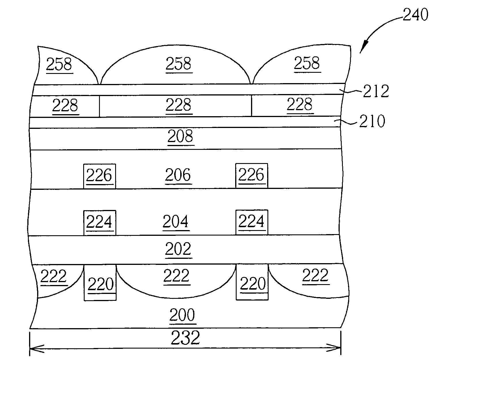
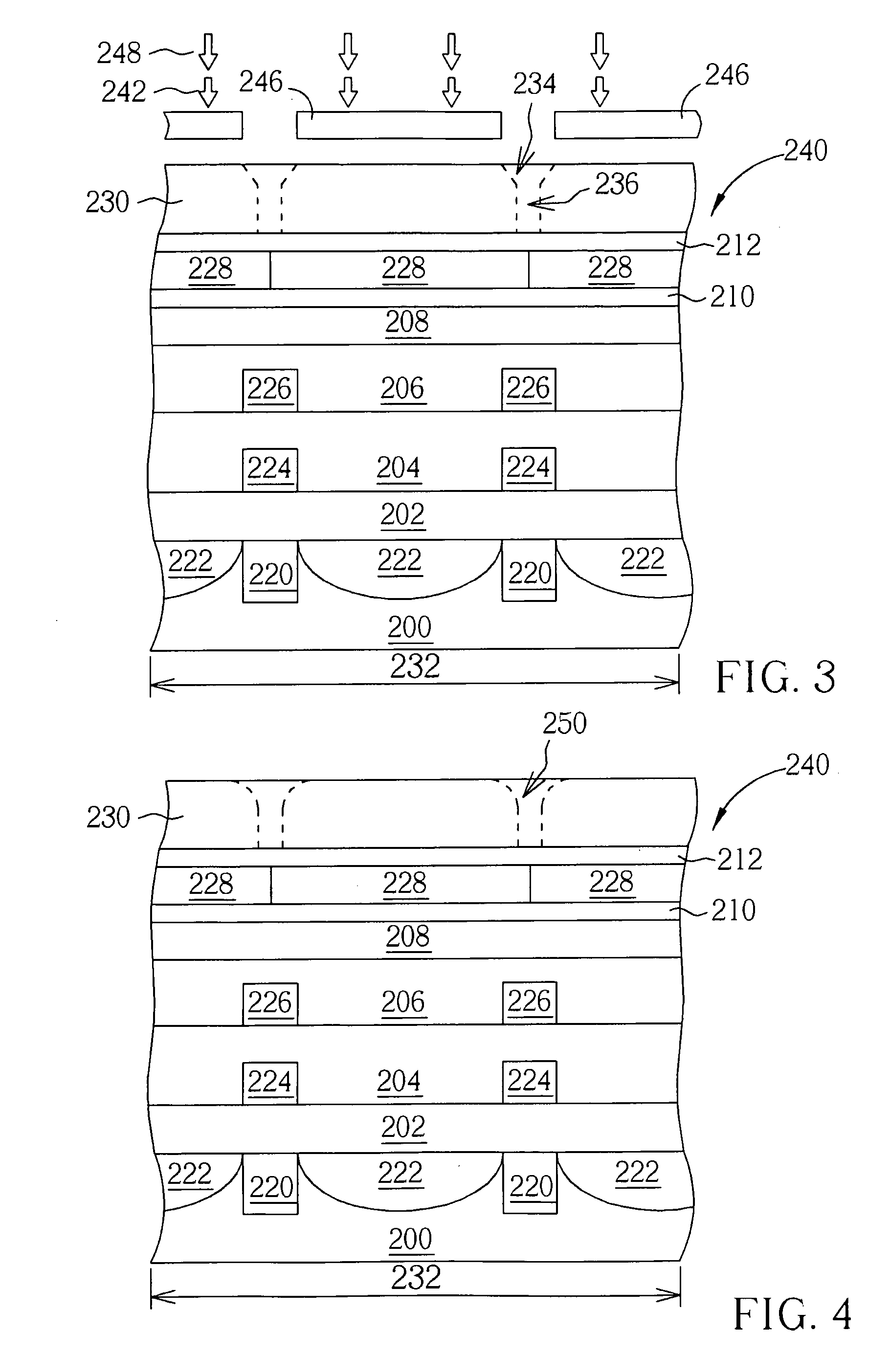
[0018]Referring to FIGS. 3-6, FIGS. 3-6 are perspective views illustrating a method for fabricating an image sensor 240 according to a preferred embodiment of the present invention. As shown in FIG. 3, a semiconductor substrate 200 is provided, in which at least a photosensitive region 232 is defined on the semiconductor substrate 200. A plurality of photodiodes 222, CMOS transistors (not shown), and shallow trench isolations 220 surrounding the photodiodes 222 are formed on the semiconductor substrate 200. Each of the photodiodes 222 is electrically connected to at least one of the transistors, and the shallow trench isolations 220 are used as an insulator between two adjacent photodiodes 222 for preventing short circuit.

[0019]Next, a planarizing layer 202 is deposited on the photodiodes 222 and the transistors, and a plurality of dielectric layers 204, 206 and patterned metal layers 224, 226 are formed on the planarizing layer 202. The metal layers 224 and 226 are formed on top of...


PUM


Abstract

A method for fabricating an image sensor is disclosed. First, a semiconductor substrate is provided, in which a photosensitive region is defined on the semiconductor substrate. At least one photosensitive material is then formed on the semiconductor substrate, and a first exposure process is performed to form a tapered pattern in the photosensitive material. A second exposure process is performed to form a straight foot pattern in the photosensitive material, and a developing process is performed to remove the tapered pattern and straight foot pattern to form the photosensitive material into a plurality of photosensitive blocks. A reflow process is conducted thereafter to form the photosensitive blocks into a plurality of microlenses.

Description

BACKGROUND OF THE INVENTION[0001]1. Field of the Invention[0002]The invention relates to a method for fabricating an image sensor.[0003]2. Description of the Prior Art[0004]As the development of digital cameras and scanners progresses, the demand for image sensor also increases accordingly. In general, today's image sensors in common usage are divided into two main categories: charge coupled device (CCD) sensors and CMO image sensors (CIS). The application of CMOS image sensors has increased significantly for several reasons. Primarily, CMOS image sensors have certain advantages of offering low operating voltage, low power consumption, and the ability for random access. Additionally, CMOS image sensors are currently capable of integration with the semiconductor fabrication process.[0005]The CMOS image sensor separates (i.e., classifies) incident light into a combination of light of different wavelengths. The light of different wavelengths is received by respective sensing elements a...

Claims


Application Information

Patent Timeline
IPC IPC(8): H01L31/0216G03F7/20
CPCG03F7/2022H01L27/14685H01L27/14643H01L27/14627
Inventor TSAI, HSIN-TINGYU, CHENG-HUNG
Owner UNITED MICROELECTRONICS CORP
Why Eureka
Eureka Blog
Learn More