Wafer level redistribution using circuit printing technology

Inactive Publication Date: 2009-12-03
AVAGO TECH WIRELESS IP SINGAPORE PTE
View PDF5 Cites 25 Cited by
  • Summary
  • Abstract
  • Description
  • Claims
  • Application Information

AI Technical Summary

Benefits of technology

[0008]Methods, systems, and apparatuses for wafer-level integrated circuit (IC) packages are described. Routing interconnects are printed onto a wafer to provide redistributed access to the I/O pads

Problems solved by technology

On some IC dies, the I/O terminals/pads are not positioned in desired locations for solder bumps/balls.
Conventional processes for forming wafer-level redistribution layers are very costly an

Method used


Image

  • Wafer level redistribution using circuit printing technology
  • Wafer level redistribution using circuit printing technology
  • Wafer level redistribution using circuit printing technology

Examples


Example

Example Embodiments

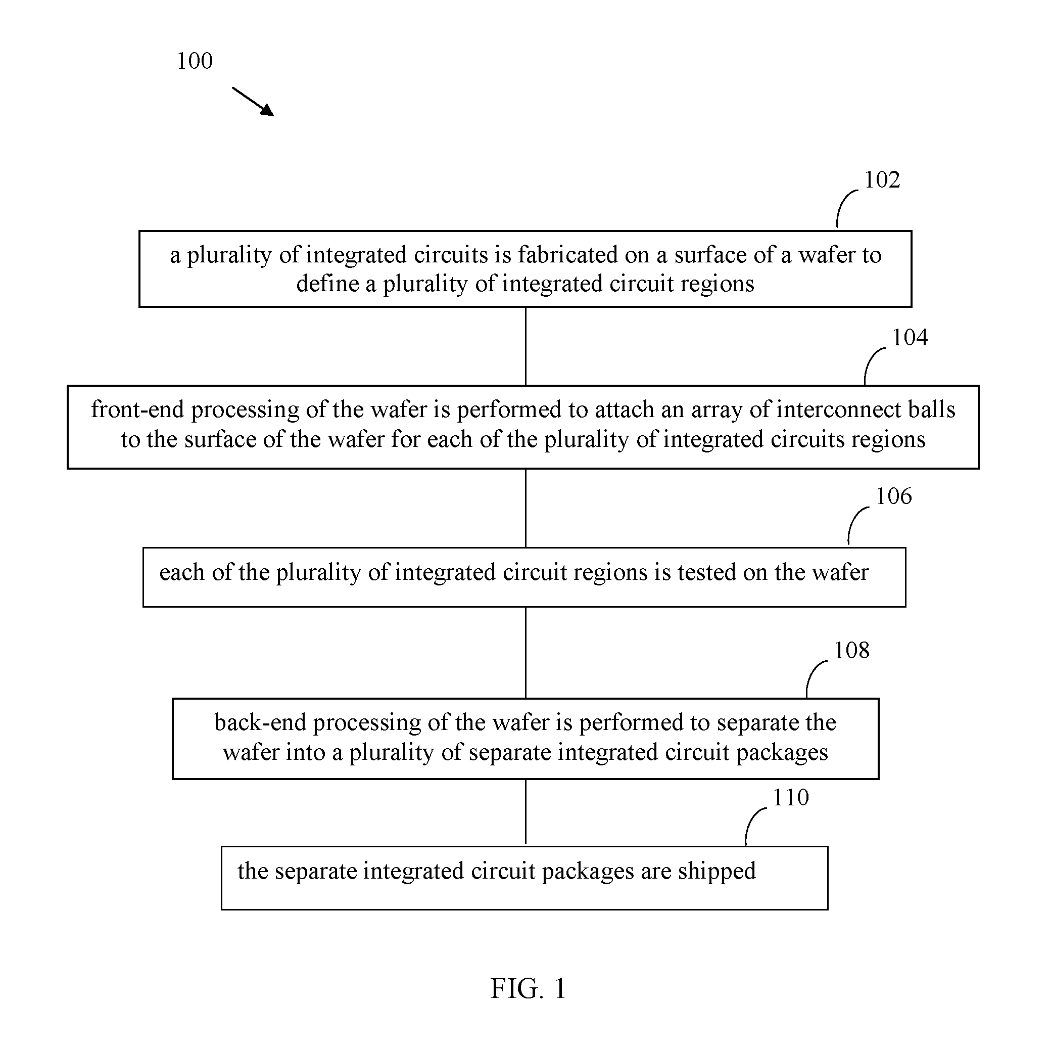
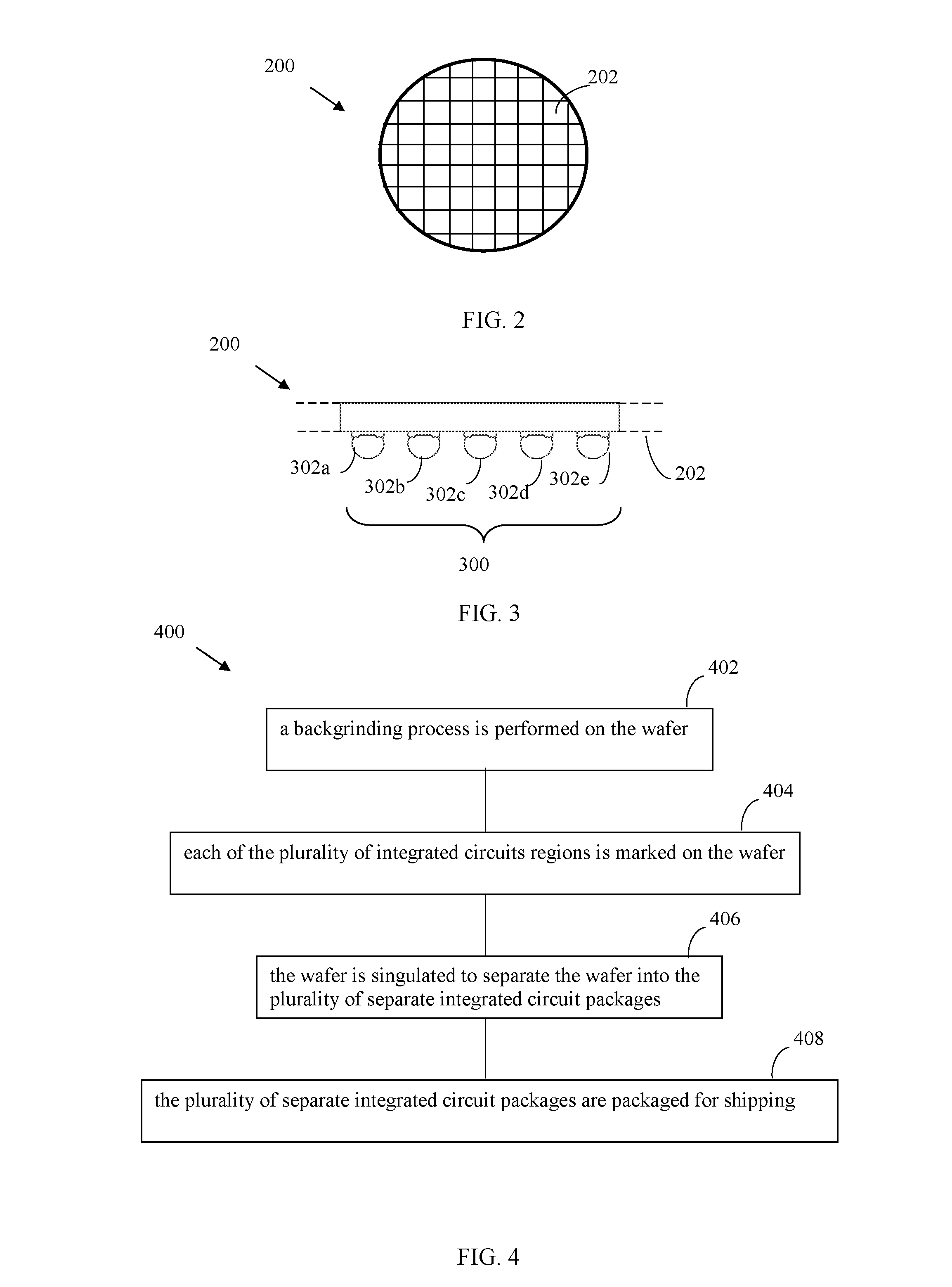
[0060]The example embodiments described herein are provided for illustrative purposes, and are not limiting. The examples described herein may be adapted to a variety of types of integrated circuit packages. Further structural and operational embodiments, including modifications / alterations, will become apparent to persons skilled in the relevant art(s) from the teachings herein.

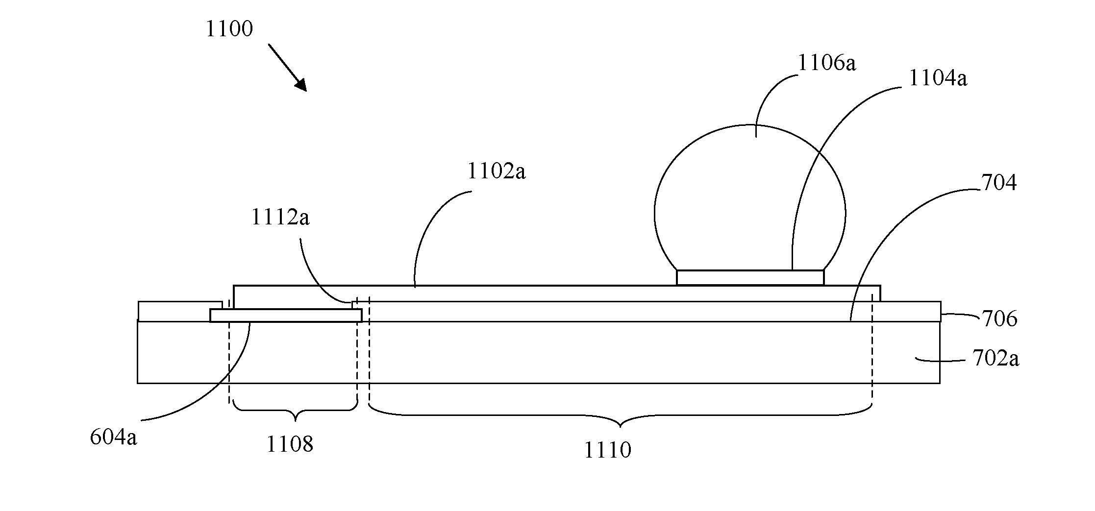
[0061]According to an embodiment, redistribution layers, also referred to as “routing interconnects,” that connect terminals of a die to bump interconnects, are formed by application of an ink material. For instance, the ink material may be applied by an ink jet printer. Such an embodiment provides for routing interconnects using a less expensive fabrication process that allows for fewer manufacturing process steps than in the fabrication processes described above for routing interconnects formed using sputtering, electroplating, and other similar processes. Furthermore, expensive masks ar...


PUM


Abstract

Methods, systems, and apparatuses for wafer-level integrated circuit (IC) packages are described. A wafer has a surface defined by a plurality of integrated circuit regions Each integrated circuit region has a passivation layer and a plurality of terminals on the surface of the wafer accessible through openings in the passivation layer. An ink jet printer is configured to print a plurality of routing interconnects on the surface of a wafer in the form of an ink. The ink jet printer is configured to print the plurality of routing interconnects such that each routing interconnect has a first portion in contact with a respective terminal of the plurality of terminals and has a second portion that extends over the passivation layer. Bump interconnects are attached to the routing interconnects. The wafer may be singulated to create a plurality of wafer-level integrated circuits.

Description

BACKGROUND OF THE INVENTION[0001]1. Field of the Invention[0002]The present invention relates to integrated circuit packaging technology, and more particularly to wafer-level ball grid array packages.[0003]2. Background Art[0004]Integrated circuit (IC) chips or dies are typically interfaced with other circuits using a package that can be attached to a printed circuit board (PCB). One such type of IC die package is a ball grid array (BGA) package. BGA packages provide for smaller footprints than many other package solutions available today. A BGA package has an array of solder ball pads located on a bottom external surface of a package substrate. Solder balls are attached to the solder ball pads. The solder balls are reflowed to attach the package to the PCB.[0005]An advanced type of BGA package is a wafer-level BGA package. Wafer-level BGA packages have several names in industry, including wafer level chip scale packages (WLCSP), among others. In a wafer-level BGA package, the solde...

Claims


Application Information

Patent Timeline
IPC IPC(8): H01L23/52H01L21/00
CPCH01L23/3114H01L2224/0401H01L24/12H01L2224/0231H01L2224/13099H01L2224/16H01L2924/01013H01L2924/01022H01L2924/01027H01L2924/01029H01L2924/01046H01L2924/01074H01L2924/01078H01L2924/01079H01L2924/01082H01L2924/14H01L2924/01033H01L2924/01047H01L23/525
Inventor HU KUNZHONG (KEVIN)
Owner AVAGO TECH WIRELESS IP SINGAPORE PTE
Why Eureka
Try Eureka