Integrated on-chip inductors and capacitors for improved performance of an optical modulator
a technology of capacitors and inductors, applied in the field of modulators, can solve the problems of reducing the bandwidth of optical output signals, affecting the performance of optical modulators, and affecting the performance of optical modulators, and reducing the amount of series inductance, which can be provided by such microstrip lines,
- Summary
- Abstract
- Description
- Claims
- Application Information
AI Technical Summary
Benefits of technology
Problems solved by technology
Method used
Image
Examples
first embodiment
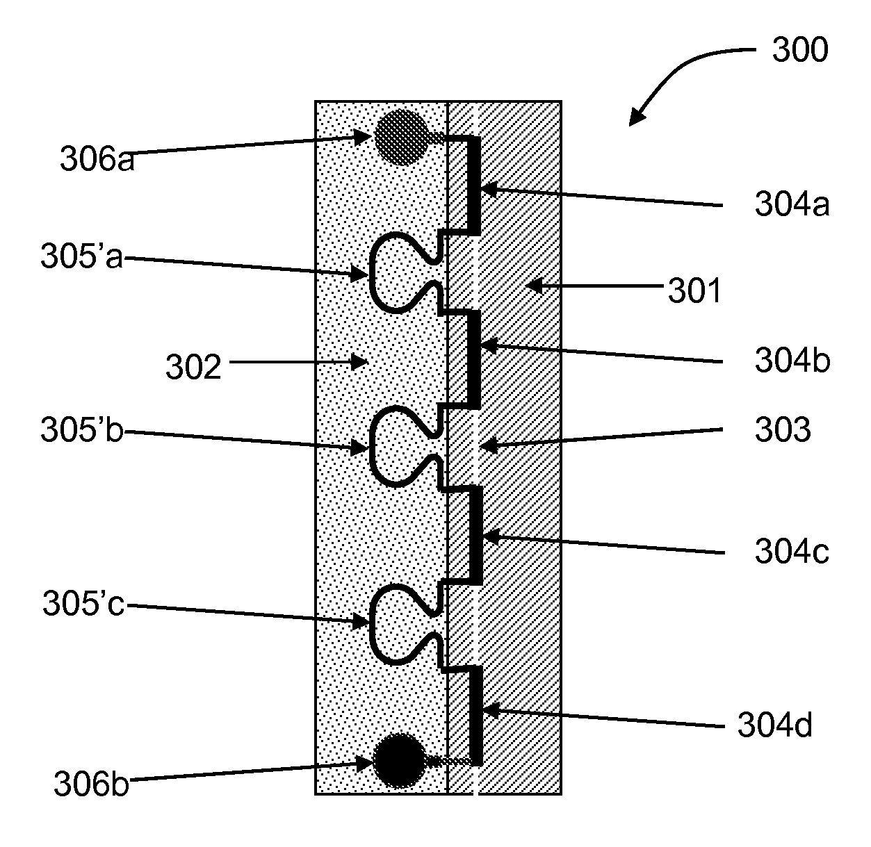
[0055]A first embodiment comprising on-chip inductors to improve modulator performance is shown in plan view in FIG. 3(a). A conducting layer 301, typically n-doped, on modulator chip 300 extends to one side from under a ridge waveguide 303 for providing a connection from an n-side of a p-n junction (310 in FIG. 3(c)) within the ridge waveguide 303 to a metal ground electrode (not shown). An insulating layer 302 extends over the rest of the modulator chip 300 up to the other side of the ridge waveguide 303. The insulating layer 302 may consist of layers of semi-insulating semiconductor materials, or layers of dielectric material, or a combinations of both. The conducting layer 301 may also extend partly or completely underneath insulating layer 302.
[0056]Conducting electrode segments 304a-d are disposed on top of the ridge waveguide 303 for providing a signal electrode connection to the p-n junction (310 in FIG. 3(c)) within the ridge waveguide 303. The length and number of the sign...
second embodiment
[0061]FIG. 3(c) is a cross-section of the second embodiment along section A-A′ in FIG. 3(b). As in FIG. 3(b), the modulator chip 300 comprises the substrate 330 with the conducting layer 301, preferably of semiconductor material, extending over a part or whole of the surface area of the substrate 330. A modulator diode 310 comprising a p-n junction within an optical ridge waveguide 303 is electrically connected to the conducting layer 301 and a traveling wave electrode 311 on top of the optical ridge waveguide 303. The modulator diode 310 layer structure may contain an intrinsic layer, single or multiple quantum wells as well as a p-type and n-type semiconductor region designed according to the required electro-optic characteristics for the modulator function.
[0062]The traveling wave electrode 311 is connected by means of the taps 312a-d or other suitable bridge contact structure to the inductors 305a-e situated on the insulating layer 302.
[0063]The substrate 330 is preferably insul...
PUM
 Abstract
Description
Claims
Application Information


