Cmos process for fabrication of ultra small or non standard size or shape semiconductor die
- Summary
- Abstract
- Description
- Claims
- Application Information
AI Technical Summary
Problems solved by technology
Method used
Image

Examples
Embodiment Construction
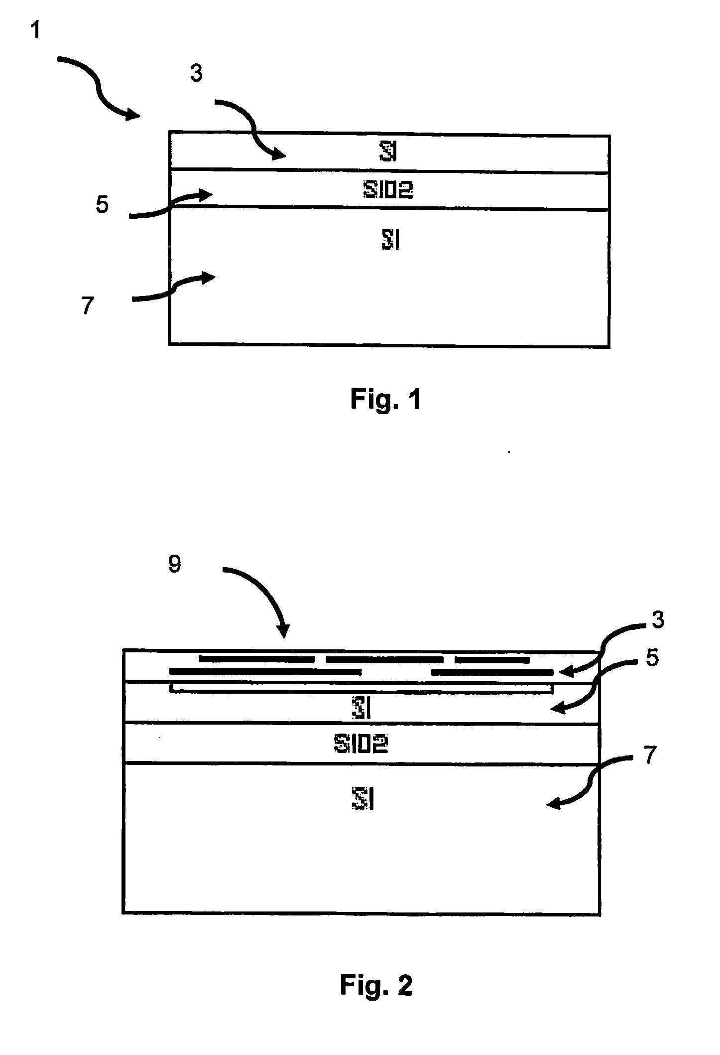
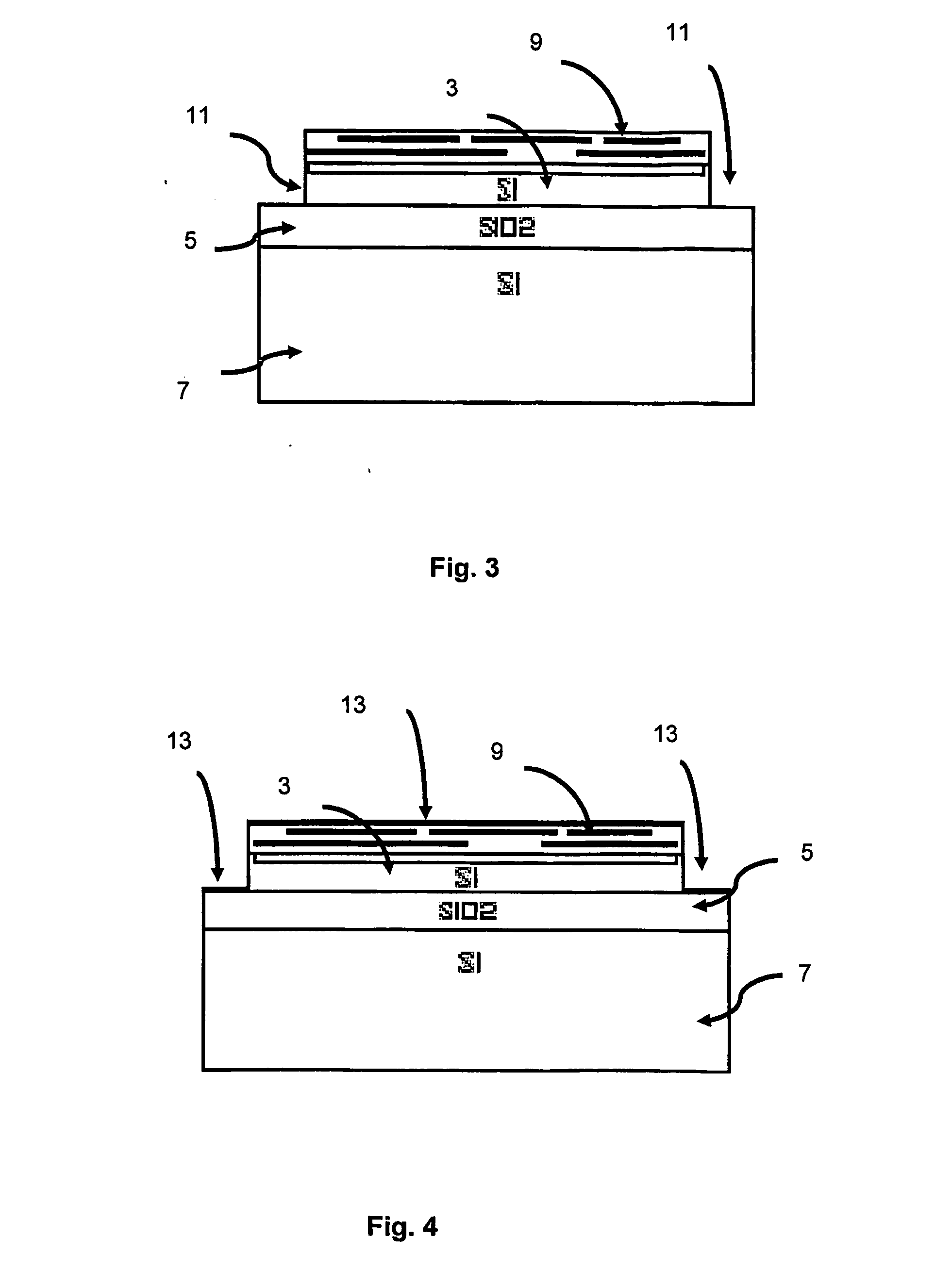
[0045]The following Figures illustrate the processing steps of the invention. For clarity, the vertical dimensions are greatly exaggerated. Although only one die is shown, it is to be understood that in the actual process there are generally a large number of similar die disposed across the wafer that are abutting the individual die depicted.
[0046]In addition, not shown are the conventional integrated circuit steps of applying photoresist, exposing the photoresist using a reticle and light to define the desired structures and removing the photoresist to open surfaces for further deposition.
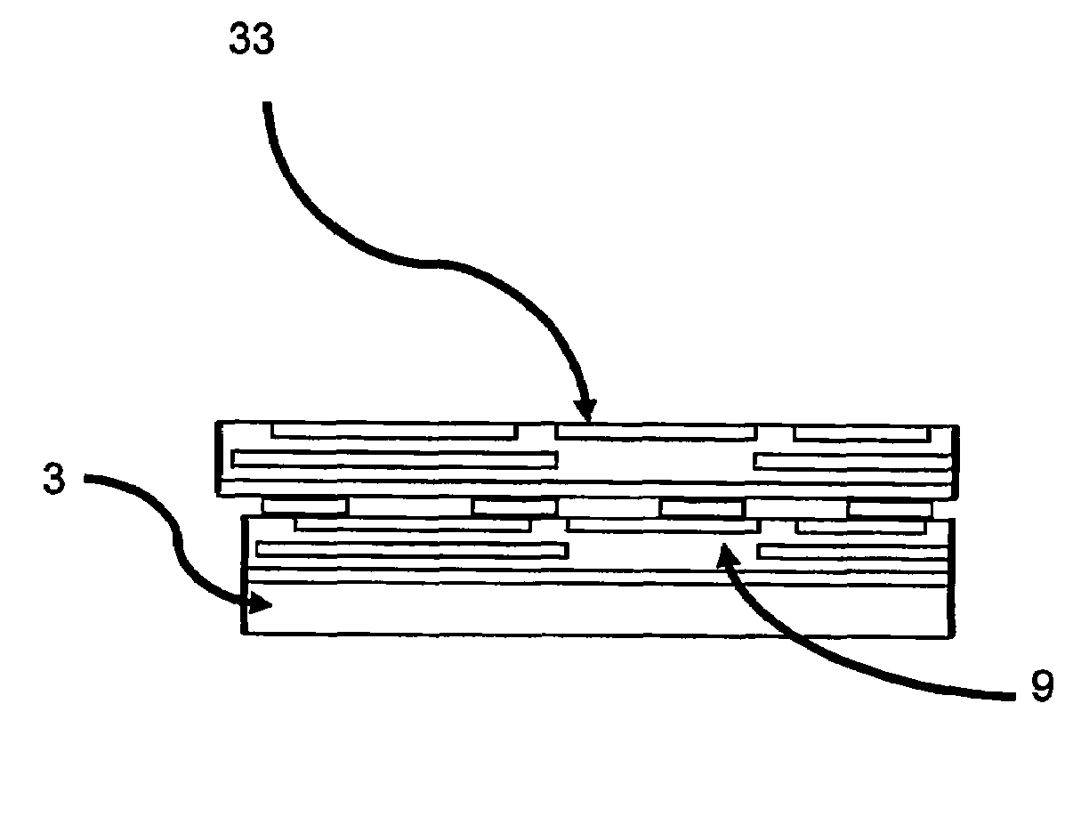
[0047]Referring to FIG. 1, Silicon on Insulator (SOI) wafer 1 starts with a top silicon layer 3 of sufficient thickness to facilitate adequate performance of the circuitry. Generally, layer 3 thickness greater or equal to 3 micro-meters is adequate. This layer also provides mechanical support for a non-standard shaped die, where as much as 25 to 50 micro-meters of silicon may be required. Semicond...
PUM
 Abstract
Description
Claims
Application Information
 - R&D Engineer
- R&D Manager
- IP Professional
- Industry Leading Data Capabilities
- Powerful AI technology
- Patent DNA Extraction
Browse by: Latest US Patents, China's latest patents, Technical Efficacy Thesaurus, Application Domain, Technology Topic.
© 2024 PatSnap. All rights reserved.Legal|Privacy policy|Modern Slavery Act Transparency Statement|Sitemap