Methods and systems for generating information to be used for selecting values for one or more parameters of a detection algorithm

a detection algorithm and information generation technology, applied in the field of methods and systems, can solve the problems of inability to predict the best output acquisition and sensitivity parameters for detecting defects on a particular wafer, the inability to detect defects of decreasing size, and the necessity of detection

Active Publication Date: 2009-12-03
KLA TENCOR TECH CORP
View PDF11 Cites 46 Cited by
  • Summary
  • Abstract
  • Description
  • Claims
  • Application Information

AI Technical Summary

Benefits of technology

[0026]FIG. 1 is a block diagram illustrating one embodiment of a computer-readable medium that includes program instructions executable on a computer system for performing one or more of the method embodiments described herein; and
[0027]FIG. 2 is a schematic diagram illustrating a side view of one embodiment of a system configured to generate information to be used for selecting values for one or more parameters of a detection algorithm.

Problems solved by technology

For instance, as the dimensions of semiconductor devices decrease, detection of defects of decreasing size has become necessary since even relatively small defects may cause unwanted aberrations in the semiconductor devices.
Although an inspection system that has adjustable output acquisition and sensitivity parameters presents significant advantages to a semiconductor device manufacturer, these inspection systems are essentially useless if the incorrect output acquisition and sensitivity parameters are used for an inspection process.
In addition, since the defects, process conditions, and noise on wafers may vary dramatically (and since the characteristics of the wafers themselves may vary dramatically), the best output acquisition and sensitivity parameters for detecting the defects on a particular wafer may be difficult, if not impossible, to predict.
Therefore, although using the correct output acquisition and sensitivity parameters will have a dramatic effect on the results of inspection, it is conceivable that many inspection processes are currently being performed with incorrect or non-optimized output acquisition and sensitivity parameters.
One problem with such methods is that it takes significant time to SEM review a single defect.
In addition, the need for multiple trips between the inspection system and the SEM adds significant time to the recipe setup.

Method used


Image

  • Methods and systems for generating information to be used for selecting values for one or more parameters of a detection algorithm
  • Methods and systems for generating information to be used for selecting values for one or more parameters of a detection algorithm

Examples


Embodiment Construction

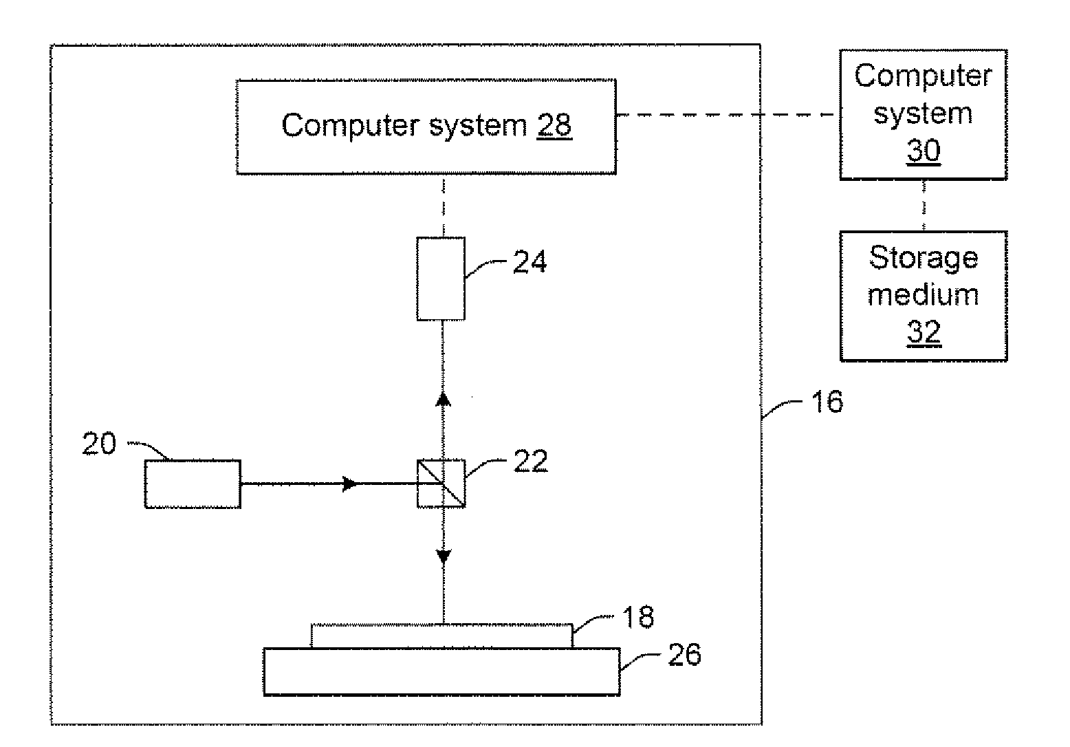
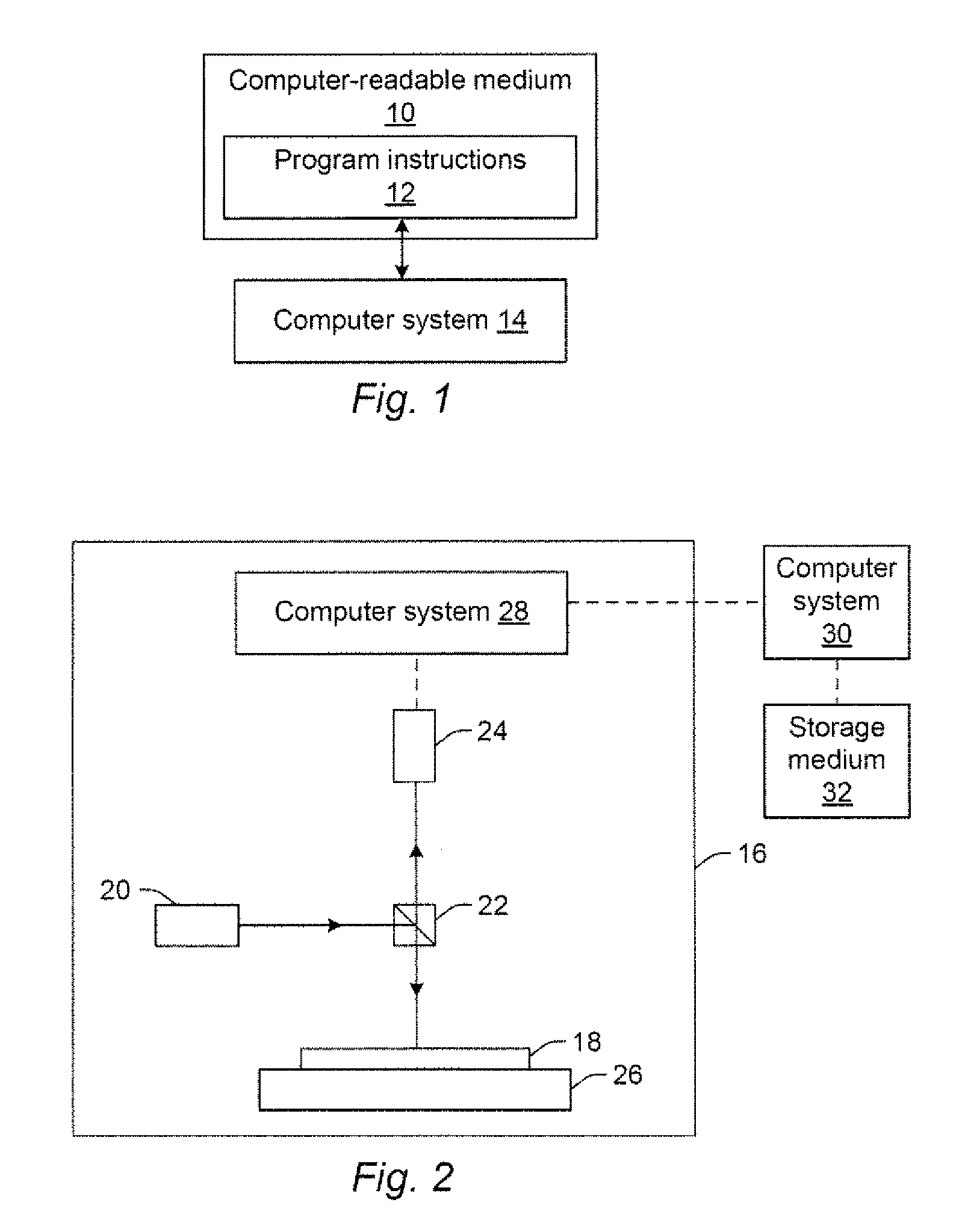
[0029]As used herein, the term “wafer” generally refers to substrates formed of a semiconductor or non-semiconductor material. Examples of such a semiconductor or non-semiconductor material include, but are not limited to, monocrystalline silicon, gallium arsenide, and indium phosphide. Such substrates may be commonly found and / or processed in semiconductor fabrication facilities.

[0030]One or more layers may be formed upon a wafer. For example, such layers may include, but are not limited to, a resist, a dielectric material, a conductive material, and a semiconductive material. Many different types of such layers are known in the art, and the term wafer as used herein is intended to encompass a wafer on which all types of such layers may be formed.

[0031]One or more layers formed on a wafer may be patterned or unpatterned. For example, a wafer may include a plurality of dies, each having repeatable patterned features. Formation and processing of such layers of material may ultimately...


PUM

PropertyMeasurementUnit
areaaaaaaaaaaa
thresholdaaaaaaaaaa
threshold offsetaaaaaaaaaa

Abstract

Methods and systems for generating information to be used for selecting values for parameter(s) of a detection algorithm are provided. One method includes without user intervention performing a scan of an area of a wafer using an inspection system and default values for parameter(s) of a detection algorithm to detect defects on the wafer. The method also includes selecting a portion of the defects from results of the scan based on a predetermined maximum number of total defects to be used for selecting values for the parameter(s) of the detection algorithm. The method further includes storing information, which includes values for the parameter(s) of the detection algorithm determined for the defects in the portion. The information can be used to select the values for the parameter(s) of the detection algorithm to be used for the inspection recipe without performing an additional scan of the wafer subsequent to the scan.

Description

BACKGROUND OF THE INVENTION[0001]1. Field of the Invention[0002]This invention generally relates to methods and systems for generating information to be used for selecting values for one or more parameters of a detection algorithm. Certain embodiments relate to generating sufficient information for selecting values for one or more parameters of a detection algorithm to be used for an inspection recipe from results of a scan of a wafer performed without user intervention and without performing an additional scan of the wafer subsequent to the scan.[0003]2. Description of the Related Art[0004]The following description and examples are not admitted to be prior art by virtue of their inclusion in this section.[0005]Fabricating semiconductor devices such as logic and memory devices typically includes processing a substrate such as a semiconductor wafer using a large number of semiconductor fabrication processes to form various features and multiple levels of the semiconductor devices. Fo...

Claims


Application Information

Patent Timeline
Patent Type & Authority Applications(United States)
IPC IPC(8): G01N21/88
CPCG01N21/9501G01N2021/8854G01N2021/8822G01N21/956
Inventor CHEN, HONGVAN RIET, MICHAEL J.LIN, JASON Z.MAHER, CHRISKOWALSKI, MICHALBECKER, BARRYCHEN, STEPHANIEBALAKRISHNAN, SUBRAMANIANTUMMALA, SURYANARAYANA
Owner KLA TENCOR TECH CORP
Why Eureka
Try Eureka