Clock signal generation apparatus
a clock signal and clock signal technology, applied in the direction of generating/distributing signals, pulse techniques, instruments, etc., can solve the problems of increasing circuit power consumption, increasing power consumption and circuit area, and sc integrator malfunction, and achieve high reliability
- Summary
- Abstract
- Description
- Claims
- Application Information
AI Technical Summary
Benefits of technology
Problems solved by technology
Method used
Image

Examples
first embodiment
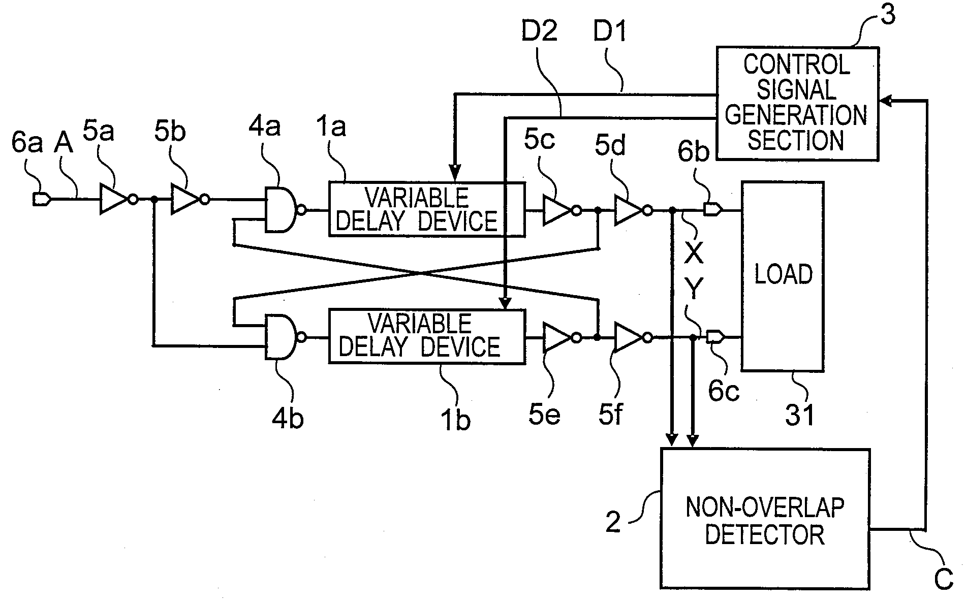
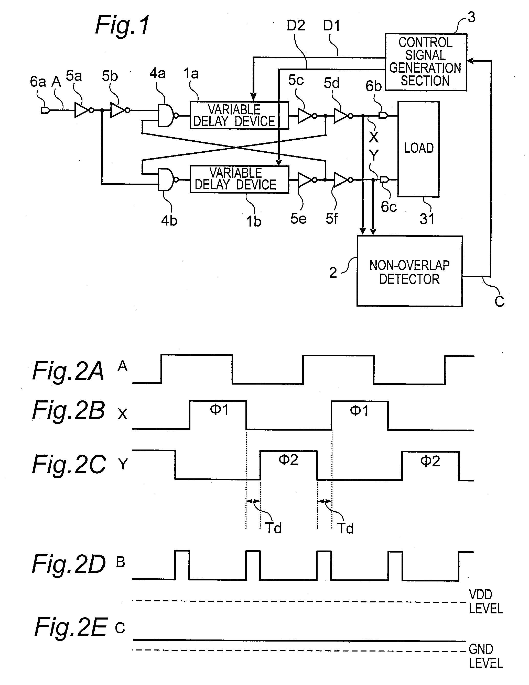
[0050]A clock signal generation apparatus according to a first embodiment of the present invention will be described below referring to FIGS. 1 to 4. FIG. 1 is a block diagram showing the configuration of a non-overlap clock signal generator serving as the clock signal generation apparatus according to the first embodiment of the present invention.
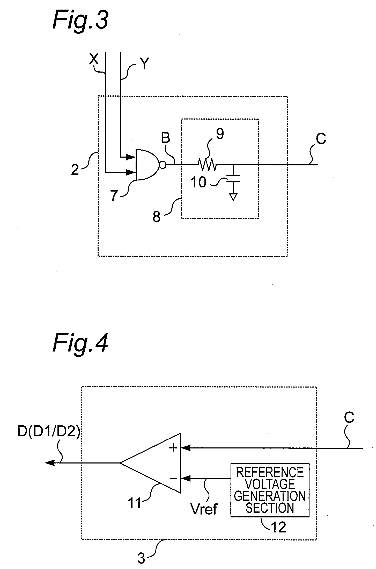
[0051]As shown in FIG. 1, the non-overlap clock signal generator according to the first embodiment contains variable delay devices 1a and 1b, a non-overlap detector 2, a control signal generation section 3, NAND logic elements 4a and 4b, inverter logic elements 5a, 5b, 5c, 5d, 5e and 5f, a clock signal input terminal 6a, an output terminal 6b for outputting a non-overlap clock signal X having phase Φ1, and an output terminal 6c for outputting a non-overlap clock signal Y having phase Φ2.
[0052]FIGS. 2A to 2E show signal waveforms in the non-overlap clock signal generator according to the first embodiment. FIG. 2A shows a clock signal A inpu...
second embodiment
[0059]Next, a non-overlap clock signal generator serving as a clock signal generation apparatus according to a second embodiment of the present invention will be described below. The basic configuration of the non-overlap clock signal generator according to the second embodiment is the same as the configuration of the non-overlap clock signal generator according to the first embodiment shown in FIG. 1 described above. Hence, in the second embodiment, components having the same functions as those of the first embodiment are designated by the same numerals, and the descriptions in the first embodiment are applied to their descriptions.
[0060]In the non-overlap clock signal generator according to the second embodiment, a variable delay device capable of adjusting the delay amount by receiving the control signal from the control signal generation section 3. FIG. 5A is a block diagram showing the configuration of a variable delay device 1 in the non-overlap clock signal generator accordin...
third embodiment
[0065]Next, a non-overlap clock signal generator serving as a clock signal generation apparatus according to a third embodiment of the present invention will be described below. Although the basic configuration of the non-overlap clock signal generator according to the third embodiment is the same as the configuration of the non-overlap clock signal generator according to the first embodiment shown in FIG. 1 described above, the configuration is different in the internal configuration of the non-overlap detector thereof. Hence, in the third embodiment, the configuration of the non-overlap detector 2A of the non-overlap clock signal generator will be described in detail, and the descriptions in the first embodiment are applied to the descriptions of the other configurations.
[0066]In the non-overlap clock signal generator according to the third embodiment, components having the same functions as those of the first embodiment are designated by the same numerals, and the descriptions in...
PUM
 Abstract
Description
Claims
Application Information