

Solar cell fabrication using implantation
a technology of solar cells and implantation, applied in the field of solar cells, can solve the problems of lack of utilization of blue light, excessive accumulation of unactivated dopants near the surface, and use of diffusion in forming dopants on the surface of semiconductor substrates, etc., and achieve the effect of low temperature annealing
- Summary
- Abstract
- Description
- Claims
- Application Information
AI Technical Summary
Benefits of technology
Problems solved by technology
Method used
Image

Examples
Embodiment Construction
[0026]In the following description, numerous details and alternatives are set forth for the purpose of explanation. However, one of ordinary skill in the art will realize that the invention can be practiced without the use of these specific details. In other instances, well-known structures and devices are shown in block diagram form in order not to obscure the description of the invention with unnecessary detail.
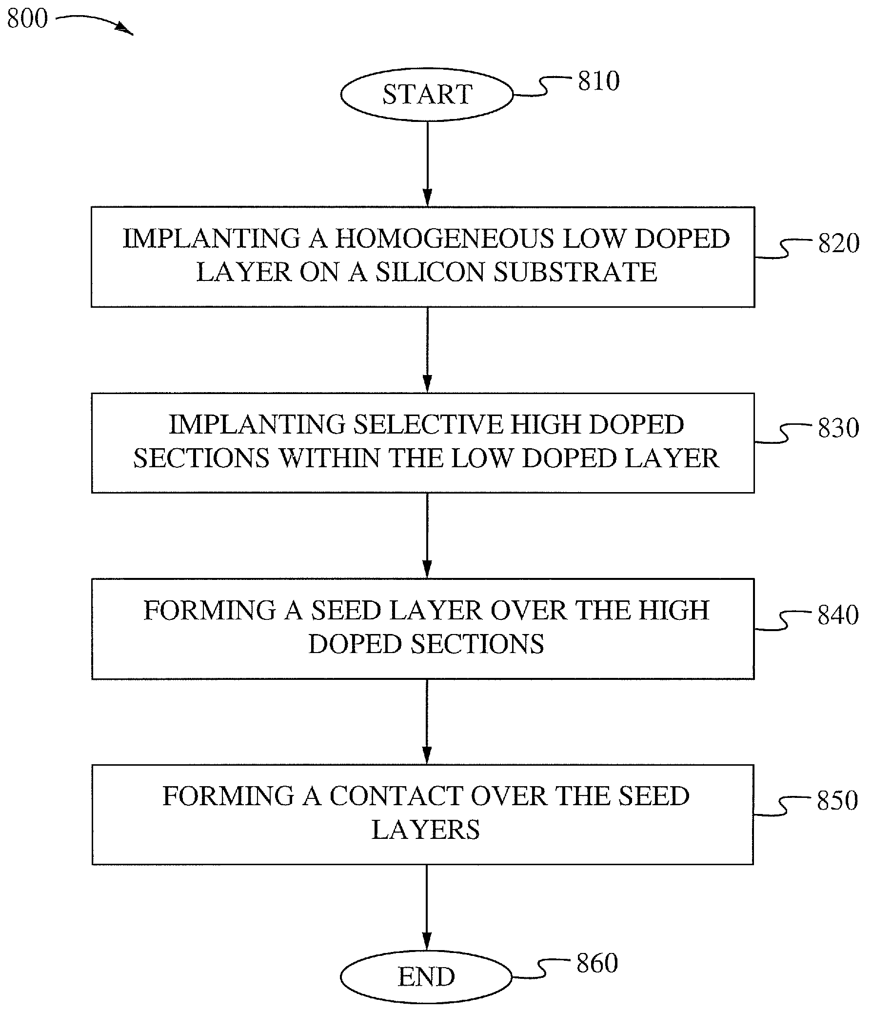
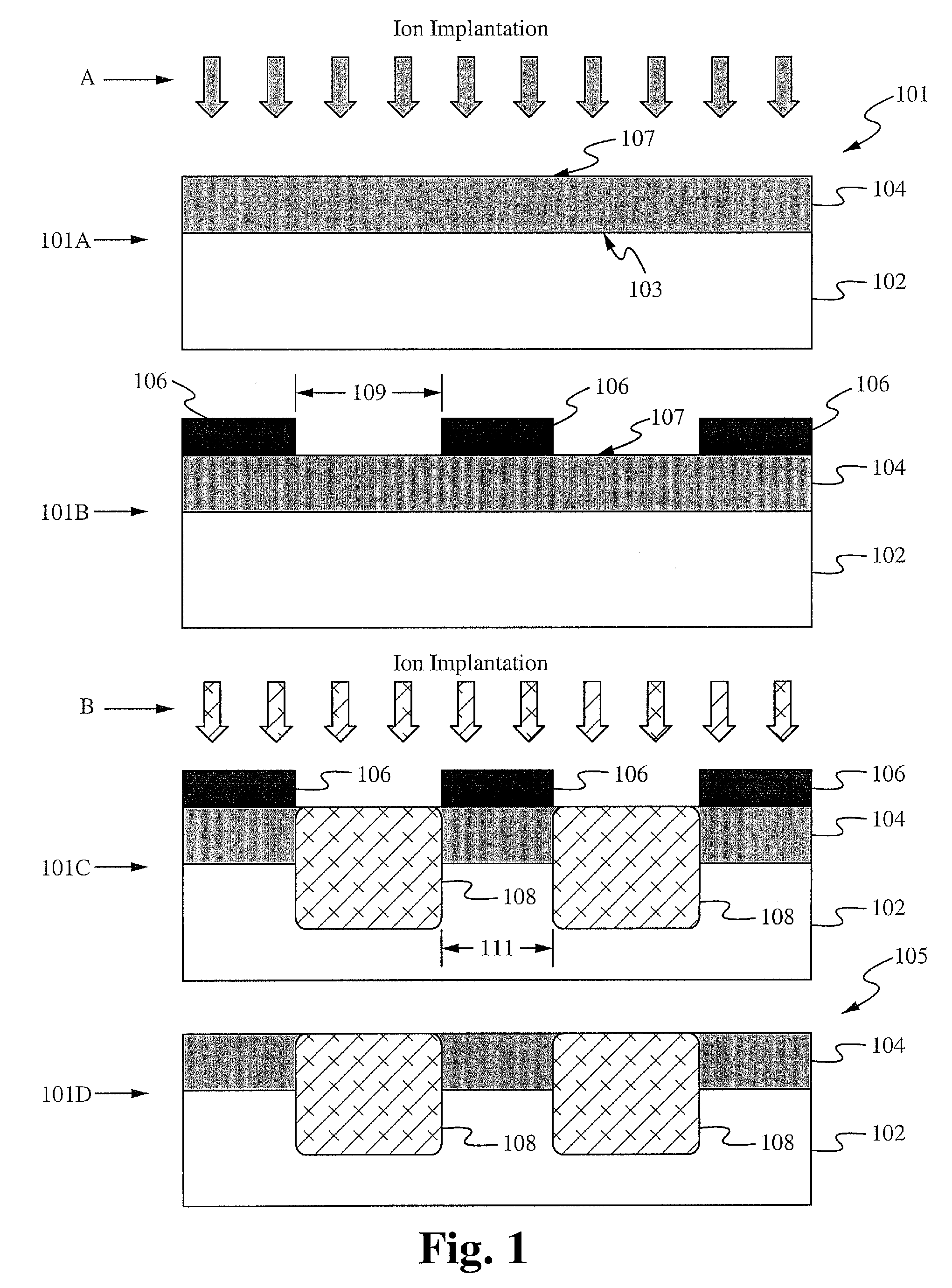
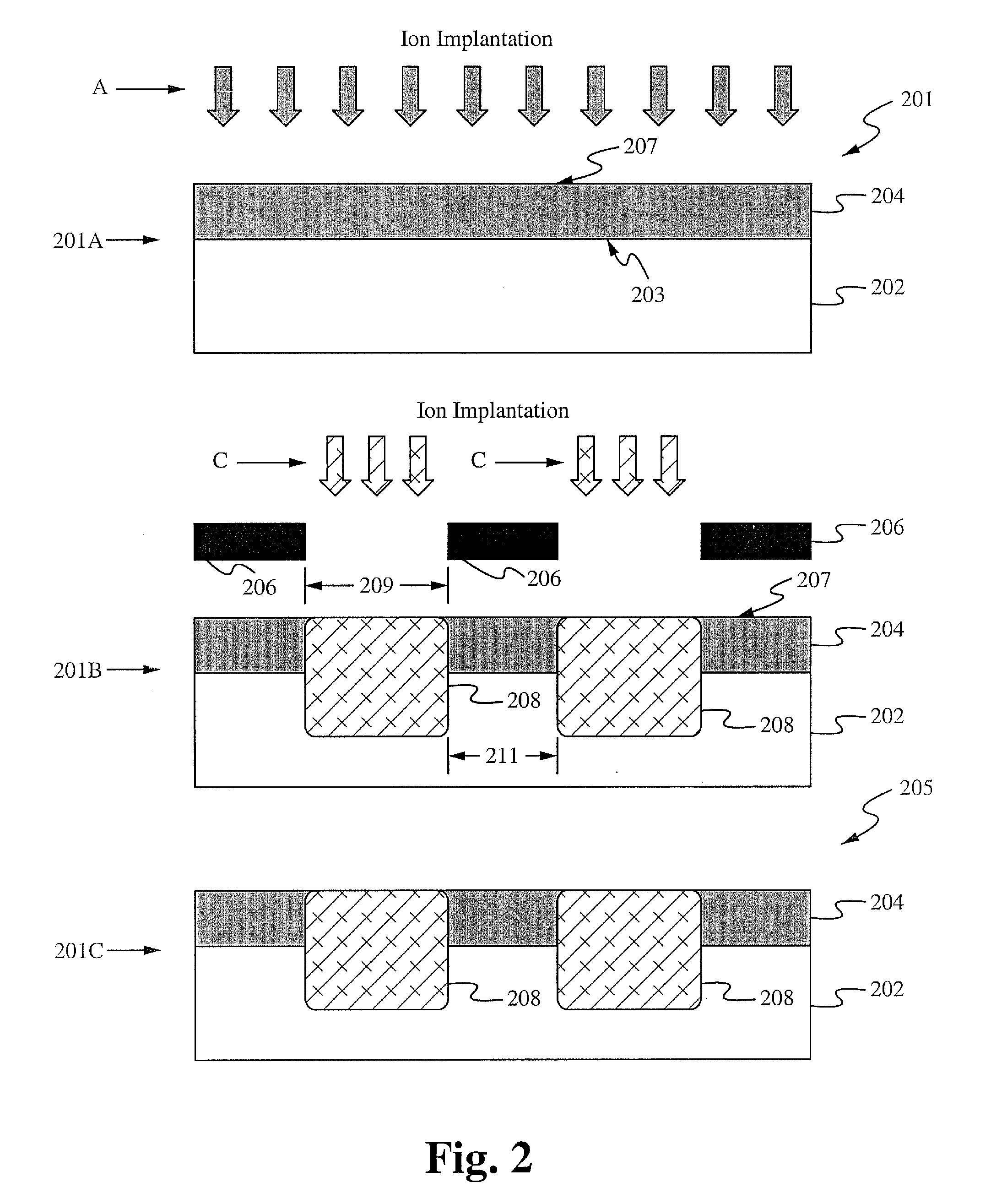
[0027]The present invention uses implantation to form homogeneous and selective emitter regions. The present invention addresses the methods for the formation of solar cells and in particular formation of a selective emitter through a series of implantation processes. Presently, such ability to manipulate and place the dopant laterally is difficult with conventional diffusion or screen printing processes. The present invention selectively controls the resistance of gridlines, contacts, and selectively controls contact resistance of a metal / semiconductor interface. Moreover,...
PUM
 Abstract
Description
Claims
Application Information