Semiconductor device and manufacturing method of the same

a semiconductor device and manufacturing method technology, applied in the direction of semiconductor devices, semiconductor/solid-state device details, electrical devices, etc., can solve the problems of reducing affecting the heat dissipation efficiency of the semiconductor device, so as to improve the heat dissipation properties of the semiconductor device and improve the manufacturing yield of the semiconductor devi

Active Publication Date: 2009-12-17
RENESAS ELECTRONICS CORP
View PDF13 Cites 93 Cited by
  • Summary
  • Abstract
  • Description
  • Claims
  • Application Information

AI Technical Summary

Benefits of technology

[0024]According to the exemplary embodiment, it is possible to improve the heat dissipation properties of the semiconductor device.
[0025]Further, it is possible to improve the manufacturing yield of the semiconductor device.

Problems solved by technology

However, these means can dissipate only about 2.5 W at best.
However, it is found that, when the heat sink (0.5 mm) having a thickness larger than the board (0.2 mm) is pasted in consideration of heat dissipation properties, the heat sink falls off due to the weight of the heat sink itself.
The falling off of the heat sink lowers the manufacturing yield of the semiconductor device.

Method used


Image

  • Semiconductor device and manufacturing method of the same
  • Semiconductor device and manufacturing method of the same
  • Semiconductor device and manufacturing method of the same

Examples


first embodiment

[0204]A semiconductor device and a manufacturing method (manufacturing process) of the same according to one embodiment of the present invention will be described with reference to the drawings.

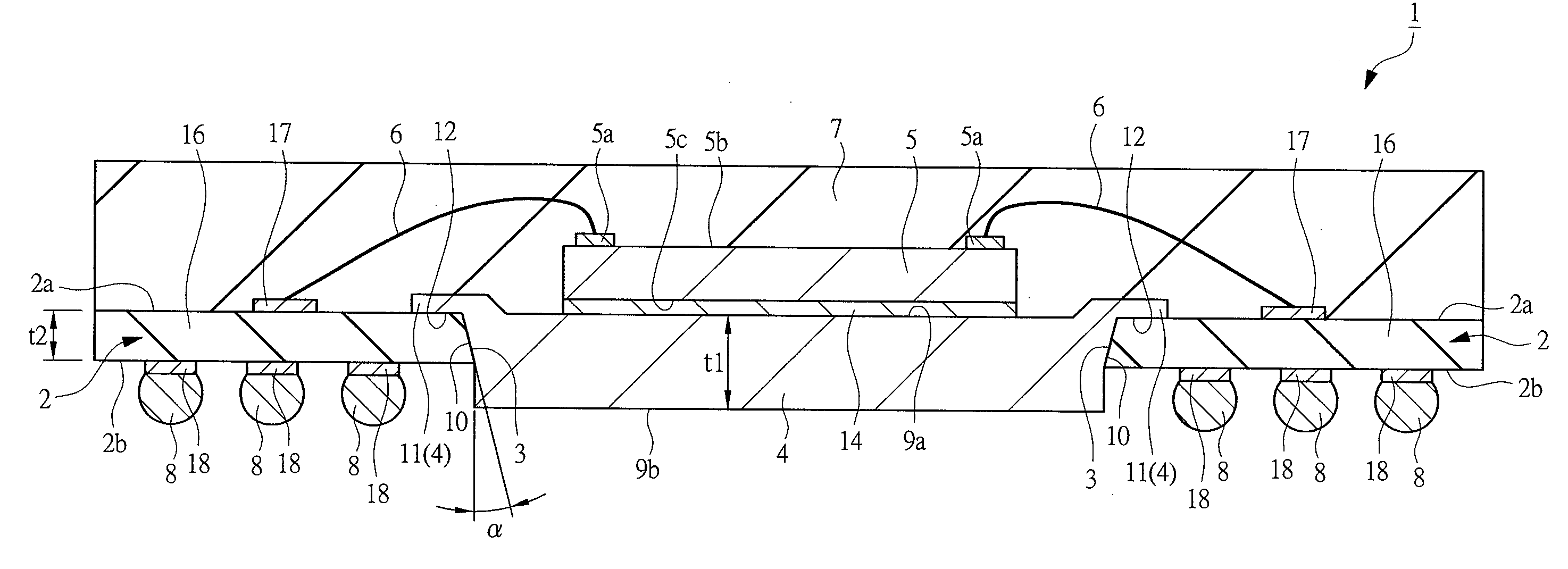
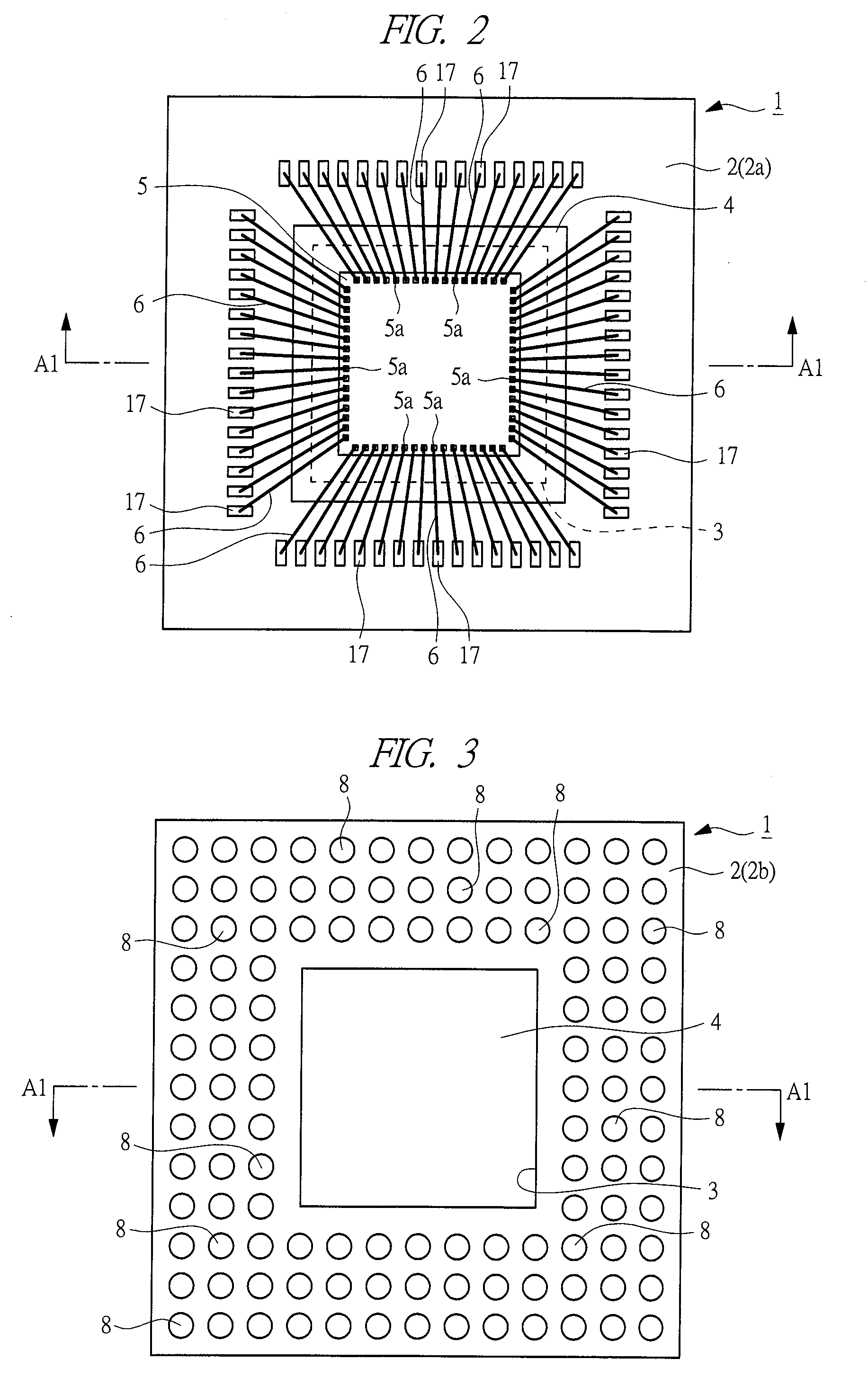
[0205]FIG. 1 is a cross-sectional view (side cross-sectional view) of a semiconductor device 1 according to one embodiment of the present invention, FIG. 2 is a perspective plan view (upper surface view) of the semiconductor device 1 when seen through a sealing resin 7, and FIG. 3 is a lower surface view (bottom view, rear view, plan view) of the semiconductor device 1. The cross-sections cut along the line A1-A1 of FIGS. 2 and 3 almost correspond to FIG. 1. Also, FIG. 4 is a cross-sectional view (side cross-sectional view) of a heat sink 4 used in the semiconductor device 1 of the present embodiment, FIG. 5 is an upper surface view (plan view) of the heat sink 4, and FIG. 6 is a lower surface view (plan view) of the heat sink 4. The cross-sections cut along the line A2-A2 of FIGS. 5 and 6 al...

second embodiment

[0305]FIGS. 48 and 49 are cross-sectional views (side cross-sectional views) of a semiconductor device 1a of the second embodiment, FIG. 50 is a perspective plan view (upper surface view) of the semiconductor device 1a when the sealing resin 7 is seen through, and FIG. 51 is a lower surface view (bottom view, rear surface view, plan view) of the semiconductor device 1a. A cross-section cut along the line A7-A7 of FIGS. 50 and 51 almost corresponds to FIG. 48, and the cross-section cut along the line A8-A8 of FIGS. 50 and 51 almost corresponds to FIG. 49. Also, FIGS. 52 and 53 are cross-sectional views (side cross-sectional views) of a heat sink 4a used in the semiconductor device 1a, FIG. 54 is an upper surface view (plan view) of the heat sink 4a used in the semiconductor device 1a, and FIG. 55 is a lower surface view (plan view) of the heat sink 4a used in the semiconductor device 1a. The cross-section cut along the line A9-A9 of FIGS. 54 and 55 corresponds to FIG. 52, and the cro...

third embodiment

[0360]FIG. 72 is a cross-sectional view (side cross-sectional view) of a semiconductor device 1b of the third embodiment, and it corresponds to FIG. 1 of the first embodiment and FIG. 48 or FIG. 49 of the second embodiment.

[0361]As shown in FIG. 72, in the semiconductor device 1b of the present embodiment, a heat sink 4b is attached to a lower surface 2b side of the wiring board 2, and the semiconductor chip 5 is mounted on an upper surface 9c of the heat sink 4b exposed at the bottom of the through-hole 3 of the wiring board 2. More specifically, the heat sink 4b is not provided with a portion corresponding to the protruded portions 11 and 11a, and has a flat plate shape (flat plate shape whose planar shape is rectangular) having the upper surface 9c and the lower surface 9d, and a pin portion (caulking portion, pin portion for caulking, caulking pin, protruded portion, convex portion) 13c is integrally provided with the heat sink 4b in the vicinity of the peripheral edge portion o...


PUM


Abstract

A semiconductor chip is mounted on a heat sink disposed inside a through-hole of a wiring board, electrodes of the semiconductor chip and connecting terminals of the wiring board are connected by bonding wires, a sealing resin is formed to cover the semiconductor chip and the bonding wires, and solder balls are formed on the lower surface of the wiring board, thereby constituting the semiconductor device. The heat sink is thicker than the wiring board. The heat sink has a protruded portion protruding to outside from the side surface of the heat sink, the protruded portion is located on the upper surface of the wiring board outside the through-hole, and the lower surface of the protruded portion contacts to the upper surface of the wiring board. When the semiconductor device is manufactured, the heat sink is inserted from the upper surface side of the wiring board.

Description

CROSS-REFERENCE TO RELATED APPLICATION[0001]The present application claims priority from Japanese Patent Application No. JP 2008-154497 filed on Jun. 12, 2008 and Japanese Patent Application No. JP 2009-6240 filed on Jan. 15, 2009, the contents of which are hereby incorporated by reference into this application.TECHNICAL FIELD OF THE INVENTION[0002]The present invention relates to a semiconductor device and a manufacturing method of the same, and more particularly to a technique effectively applied to a semiconductor package having improved heat dissipation properties and a manufacturing method of the same.BACKGROUND OF THE INVENTION[0003]A semiconductor device of a BGA package configuration is manufactured by mounting a semiconductor chip on a wiring board, electrically connecting electrodes of the semiconductor chip and connecting terminals of the wiring board by bonding wires, sealing the semiconductor chip and the bonding wires with resin, and connecting solder balls on a rear s...

Claims


Application Information

Patent Timeline
Patent Type & Authority Applications(United States)
IPC IPC(8): H01L23/34H01L21/50
CPCH01L21/561H01L2224/32225H01L23/4334H01L24/83H01L24/97H01L2224/32145H01L2224/48091H01L2224/48227H01L2224/49171H01L2224/73265H01L2224/83192H01L2224/838H01L2224/92247H01L2224/97H01L2924/01029H01L2924/01047H01L2924/01057H01L2924/01074H01L2924/01075H01L2924/01078H01L2924/01079H01L2924/01082H01L2924/14H01L2924/15311H01L2924/19043H01L23/3128H01L2224/32245H01L2224/45144H01L24/49H01L2924/0665H01L2924/014H01L2924/01033H01L2924/01006H01L2924/01005H01L2224/2919H01L24/48H01L2924/00014H01L2224/85H01L2224/83H01L2924/00H01L2924/3512H01L2924/00012H01L2924/351H01L2924/181H01L24/45H01L2224/05554H01L24/73H01L2924/10162H01L2224/05599
Inventor TAKAHASHI, NORIYUKISHISHIDO, MAMORU
Owner RENESAS ELECTRONICS CORP
Why Eureka
Try Eureka