Multilayer ceramic electronic component and method for manufacturing the same

a technology of electronic components and ceramics, applied in the direction of fixed capacitors, variable capacitors, fixed capacitor details, etc., can solve the problems of increasing the area of ceramic layers within the predetermined size standards of products, and achieving high bonding strength and efficient manufacturing of multi-layer ceramic electronic components

Active Publication Date: 2009-12-17
MURATA MFG CO LTD
View PDF25 Cites 27 Cited by
  • Summary
  • Abstract
  • Description
  • Claims
  • Application Information

AI Technical Summary

Benefits of technology

[0010]To overcome the problems described above, preferred embodiments of the present invention provide a high-performance small multilayer ceramic electronic component having a thin external terminal electrode with high bonding strength to a ceramic body and a method for efficiently manufacturing the multilayer ceramic electronic component.

Problems solved by technology

However, a short circuit between internal electrodes is more likely to occur as the thickness of ceramic layers decreases.
This causes problems with quality assurance.
However, increasing the area of ceramic layers within the predetermined size standards of products has its limit, and the thickness of external terminal electrodes prevents the area of ceramic layers from being widened.
However, a thick conductive paste easily adheres to the central portion of the end of the ceramic body with this method due to viscosity of the conductive paste.
Although the high bonding strength of an external terminal electrode to a ceramic body due to an adhesive effect of glass is achieved in the existing method for applying a conductive paste and baking it, such high bonding strength cannot be achieved in the method for forming an external terminal electrode by direct plating.
Therefore, the bonding strength of an external terminal electrode defined by a plating film to a ceramic body tends to be insufficient, which causes a problem of low reliability.

Method used


Image

  • Multilayer ceramic electronic component and method for manufacturing the same
  • Multilayer ceramic electronic component and method for manufacturing the same
  • Multilayer ceramic electronic component and method for manufacturing the same

Examples


first preferred embodiment

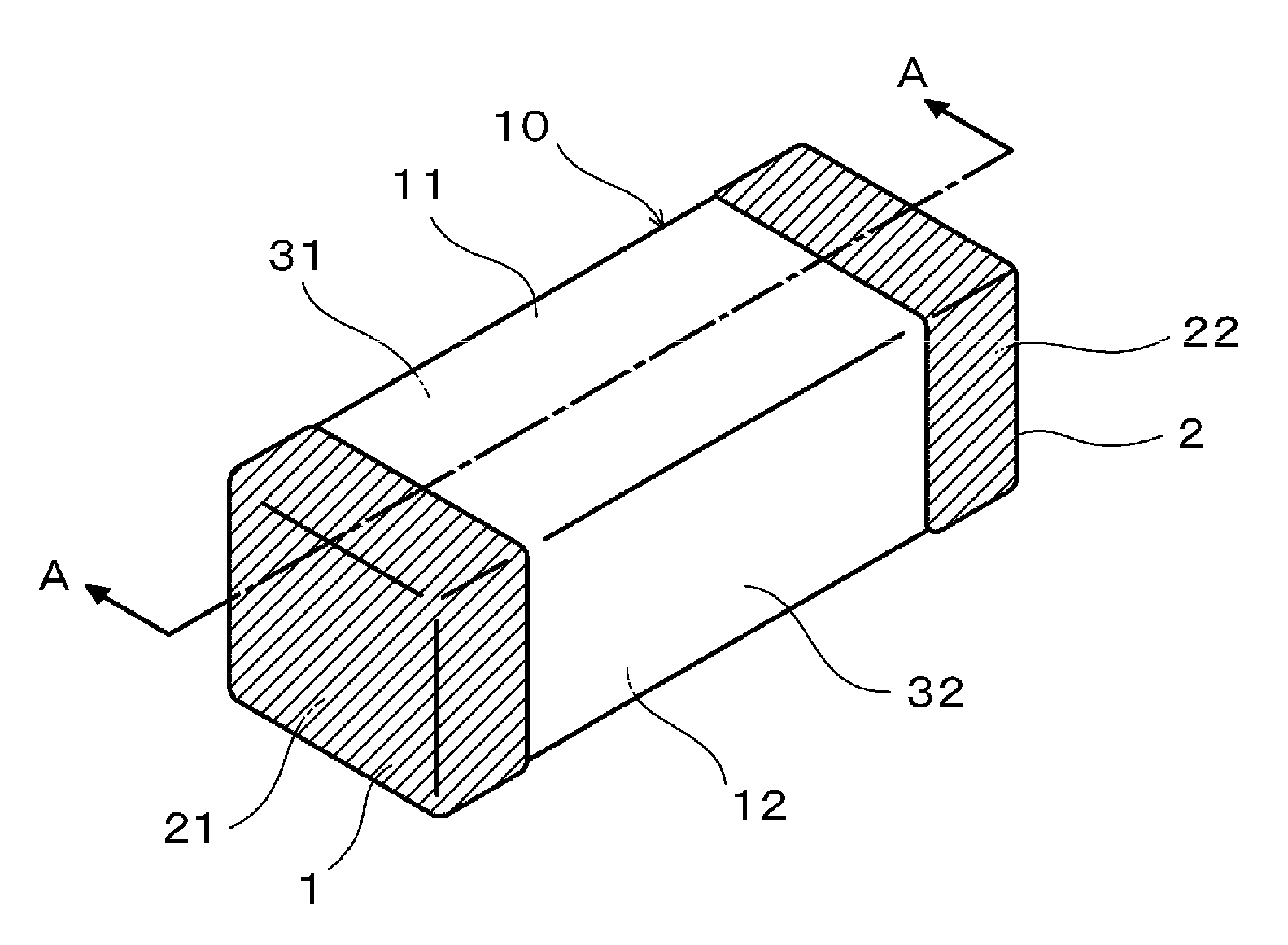
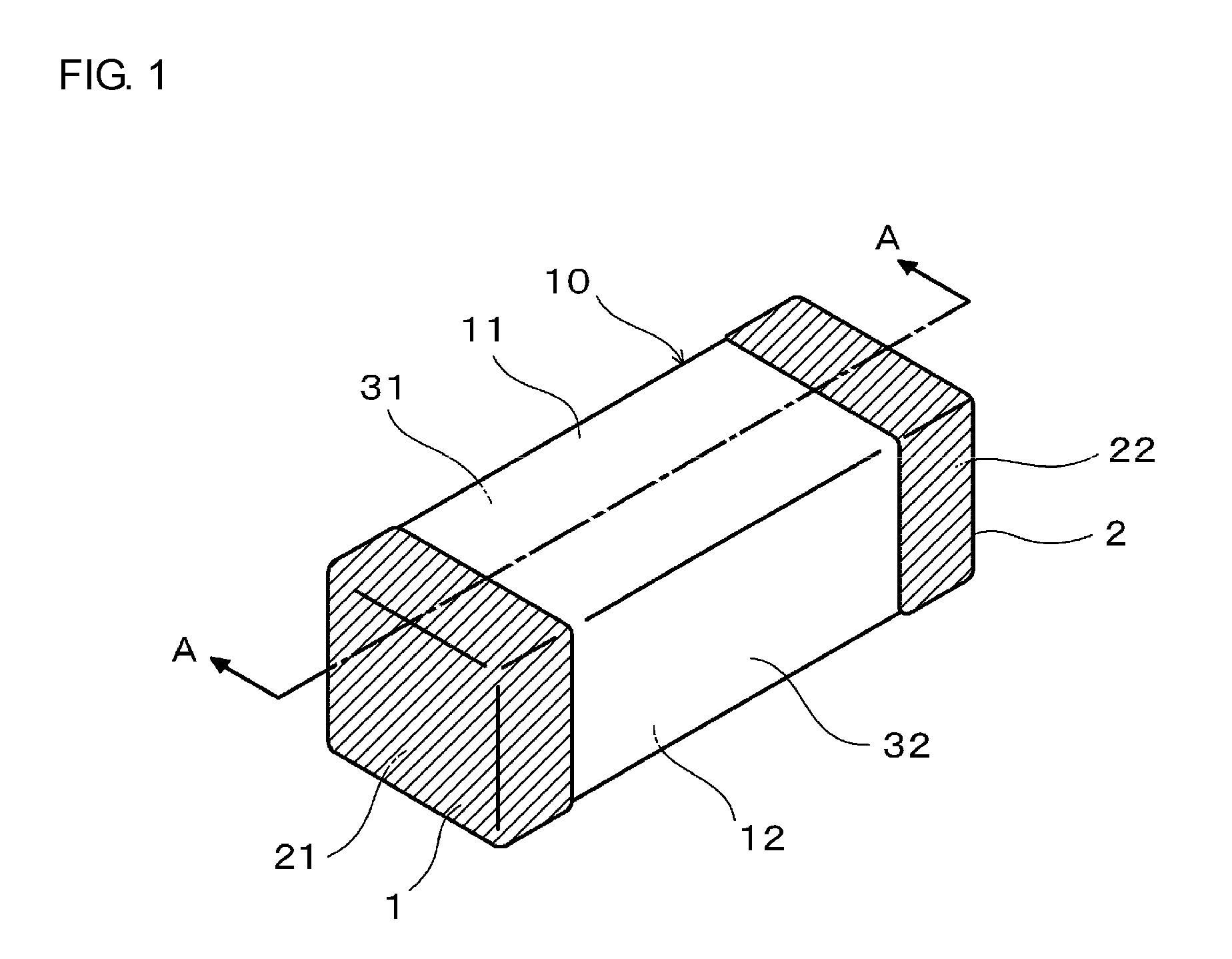
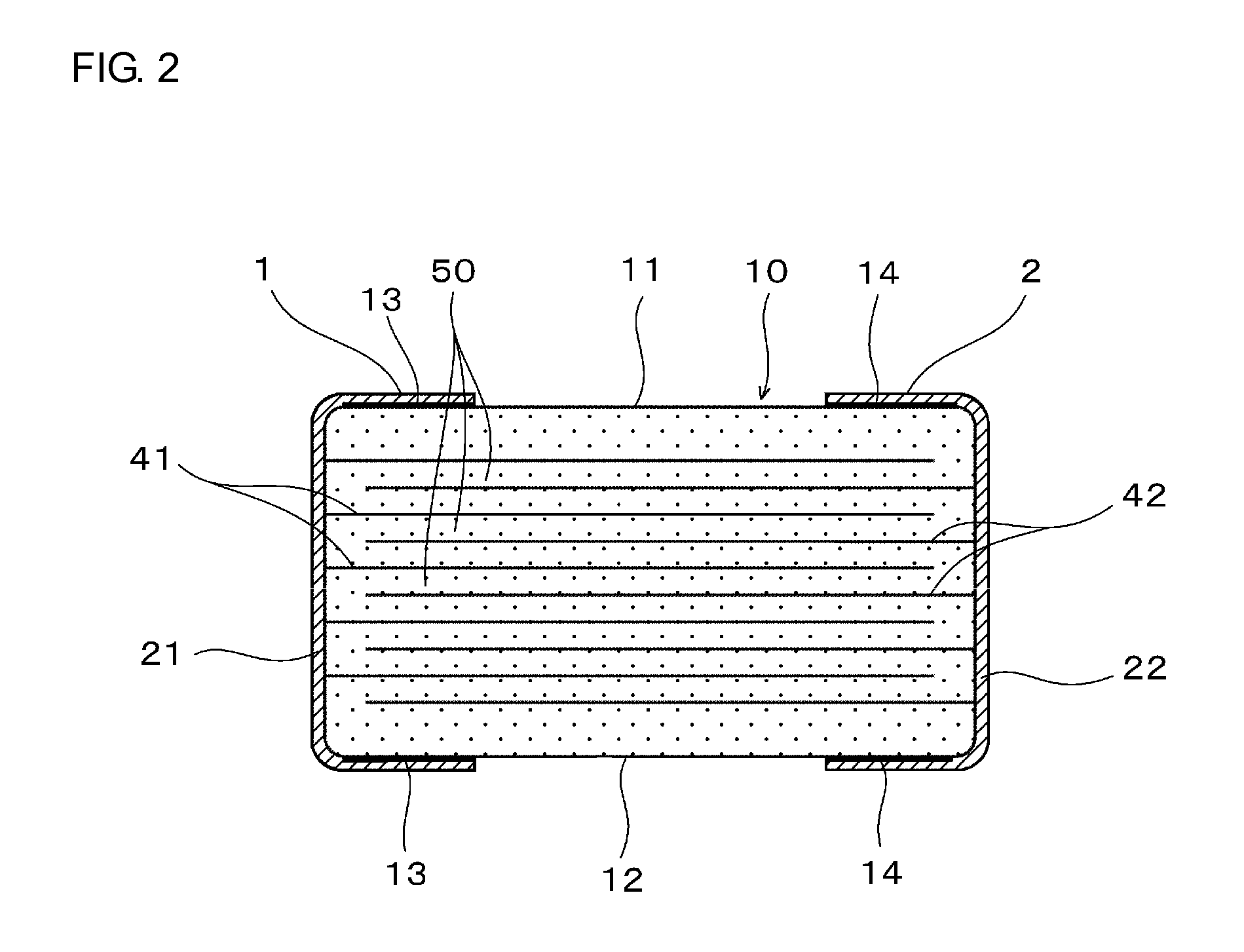
[0031]FIG. 1 is a perspective view showing a multilayer ceramic electronic component according to a first preferred embodiment of the present invention. FIG. 2 is a sectional view taken along line A-A of FIG. 1. FIG. 3 is a fragmentary enlarged view of FIG. 2 showing a film structure of a first external terminal electrode. FIG. 4 is a schematic exploded plan view of FIG. 1.

[0032]As shown in FIGS. 1 and 2, the multilayer ceramic electronic component includes a substantially rectangular parallelepiped ceramic body 10 having a first principal surface 11 and a second principal surface 12 opposing each other, and a first side surface 21, a second side surface 22, a third side surface 31, and a fourth side surface 32 connecting the first principal surface 11 to the second principal surface 12. The ceramic body 10 includes a plurality of stacked ceramic layers 50.

[0033]The first side surface 21 and the second side surface 22 oppose each other, and the third side surface 31 and the fourth s...

second preferred embodiment

[0080]FIG. 7 shows a multilayer ceramic electronic component according to a second preferred embodiment of the present invention. The multilayer ceramic electronic component according to the second preferred embodiment has substantially the same structure as the multilayer ceramic electronic component according to the first preferred embodiment, except that the ceramic body 10 further includes first dummy inner conductors D1 having exposed portions on the first side surface 21 and second dummy inner conductors D2 having exposed portions on the second side surface 22. In FIG. 7, the portions designated by the same reference numerals as those in FIGS. 2 and 4 represent the same portions or the corresponding portions.

[0081]Both of the first and second dummy inner conductors D1 and D2 are electrodes that do not contribute to the electrical characteristics.

[0082]The first dummy inner conductors D1 are preferably formed on the same planes as the second inner conductors 42, and are also di...

third preferred embodiment

[0087]FIG. 8 shows an array type multilayer ceramic electronic component (capacitor array) according to a third preferred embodiment of the present invention. FIG. 9 shows an arrangement of the inner conductors. The array type multilayer ceramic electronic component of the third preferred embodiment includes a substantially rectangular parallelepiped capacitor array body (ceramic body) 10A having first and second principal surfaces 11 and 12 opposing each other, first and second side surfaces 21 and 22 opposing each other, and third and fourth side surfaces 31 and 32 opposing each other.

[0088]A plurality of first external terminal electrodes 101 are provided on the first side surface 21 of the capacitor array body 10A. A plurality of second external terminal electrodes 102 are provided on the second side surface 22. The first external terminal electrodes 101 and the second external terminal electrodes 102 are electrically insulated.

[0089]Inside the capacitor array body 10A, as shown...


PUM

PropertyMeasurementUnit
thicknessaaaaaaaaaa
thicknessaaaaaaaaaa
heightaaaaaaaaaa

Abstract

A multilayer ceramic electronic component includes external terminal electrodes that are formed by direct plating on the first and second side surfaces of a ceramic body including stacked ceramic layers and inner conductors. The external terminal electrodes include base plating films formed so as to cover the exposed portions of inner conductors. Voids are provided that are open to the side surfaces of the ceramic body so as to be adjacent to the ends in the width direction of the exposed portions of the inner conductors. A plating metal defining the base plating films enters the voids and is electrically connected to the inner conductors in the ceramic body.

Description

BACKGROUND OF THE INVENTION[0001]1. Field of the Invention[0002]The present invention relates to a multilayer ceramic electronic component and a method for manufacturing the multilayer ceramic electronic component. Particularly, the present invention relates to a multilayer ceramic electronic component in which an external terminal electrode connected to an inner conductor is formed on the surface of a ceramic body by direct plating and a method for manufacturing the multilayer ceramic electronic component.[0003]2. Description of the Related Art[0004]In recent years, the market for small portable electronic devices such as cellular phones, notebook computers, digital cameras, and digital audio devices has expanded. Portable electronic devices with not only smaller sizes but also higher performance have been rapidly developed. Such portable electronic devices include many multilayer ceramic electronic components. For such multilayer ceramic electronic components, smaller sizes and hi...

Claims


Application Information

Patent Timeline
Patent Type & Authority Applications(United States)
IPC IPC(8): H01G4/228H01G4/005
CPCH01G4/012H01G4/232Y10T29/435H01G4/30H01G4/2325
Inventor TASHIMA, TAKESHIMATSUMOTO, HIROYUKI
Owner MURATA MFG CO LTD
Why Eureka
Try Eureka