Characterizing Thermomechanical Properties of an Organic Substrate Using Three-Dimensional Finite Element Analysis

a technology of finite element analysis and thermomechanical properties, applied in the field of electric and electronic devices, can solve the problems of low accuracy of warp prediction, low accuracy low reliability of organic chip carrier, etc., and achieve the effect of facilitating the best representation

Inactive Publication Date: 2009-12-17
GLOBALFOUNDRIES INC
View PDF1 Cites 23 Cited by
  • Summary
  • Abstract
  • Description
  • Claims
  • Application Information

AI Technical Summary

Benefits of technology

[0010]Illustrative embodiments of the present invention provide techniques for accurate warp projection of an organic chip carrier (substrate). Embodiments of the invention circumvent the need for a laminate theory approach by launching a thre

Problems solved by technology

These current prediction methods lead to a warp prediction that is often inaccurate, and thus not very useful.
Ultimately, these inaccuracies result in organic chip carriers that are higher in cost and/or less reliable than desired.
This can occur, for example, when an integrated circuit (IC) chip cannot be joined to the chip site due to poor chip site co-planarity.
In other words, a flat chip cannot be joined to a non-flat substrate because interconnections may be misaligned causing electrical open-circuits.
Another manifestation of poor warp prediction is where, due at least in part to warp of the chip carrier, some inputs/outputs (I/O) of th

Method used


Image

  • Characterizing Thermomechanical Properties of an Organic Substrate Using Three-Dimensional Finite Element Analysis
  • Characterizing Thermomechanical Properties of an Organic Substrate Using Three-Dimensional Finite Element Analysis
  • Characterizing Thermomechanical Properties of an Organic Substrate Using Three-Dimensional Finite Element Analysis

Examples


Embodiment Construction

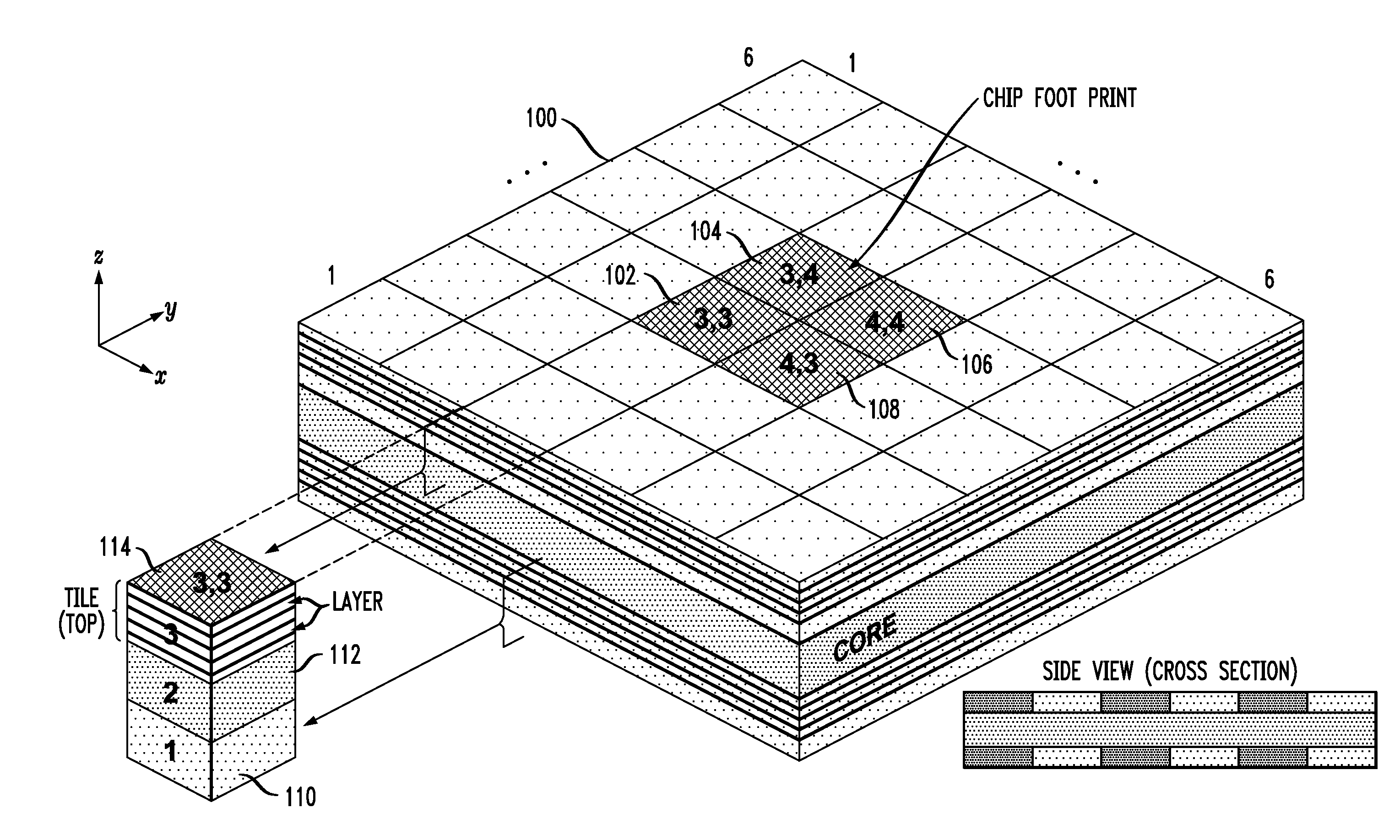
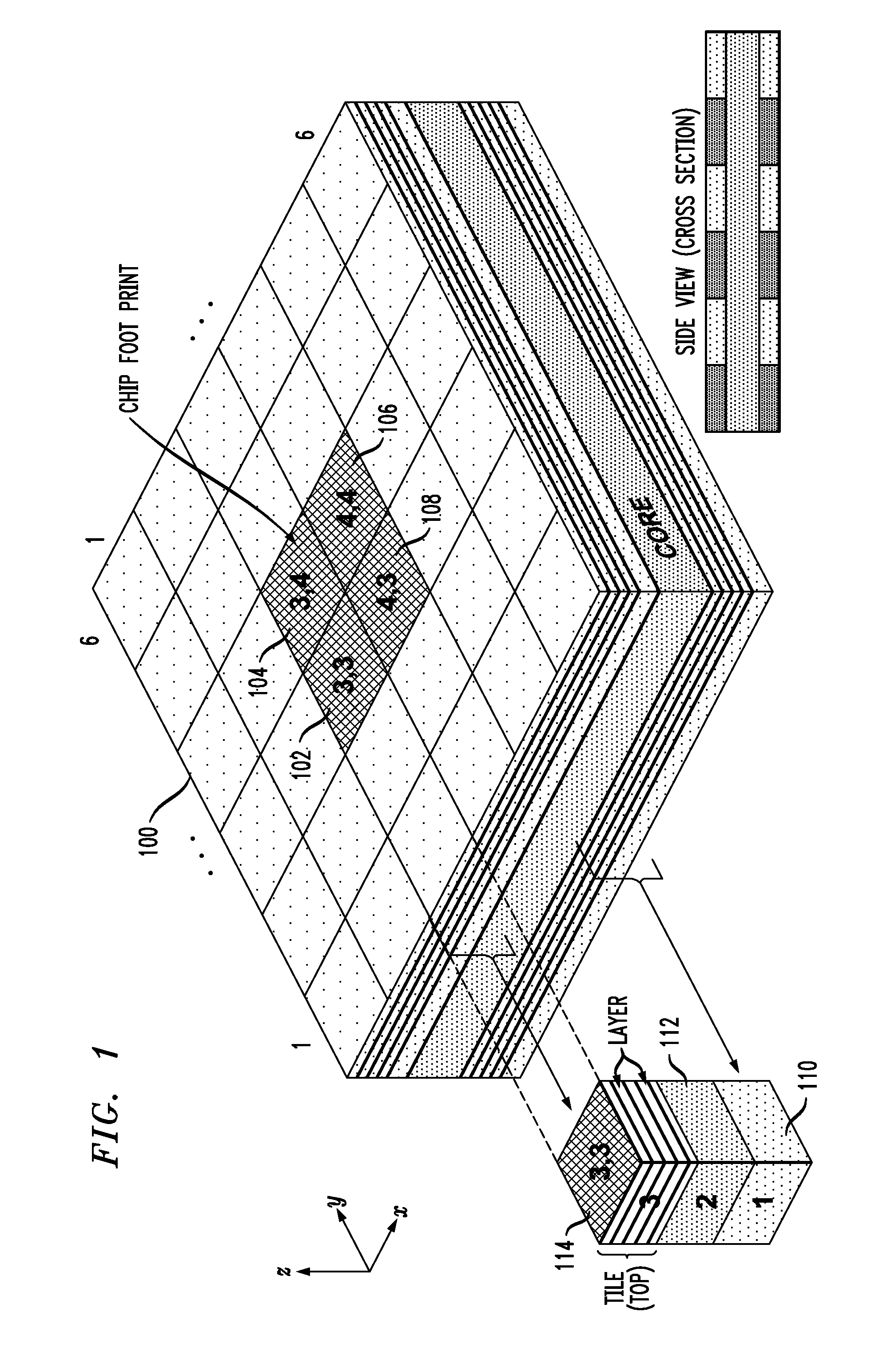
[0030]The present invention will be described herein in the context of illustrative methodologies using 3-D FEM for improving the prediction of warp in an organic chip carrier or substrate. Embodiments of the invention divide the substrate into a plurality of “tiles” and then generate a 3-D FEM geometry for each tile from 2-D images respective circuit layers of the tile. This methodology mimics an actual substrate manufacturing process, and facilitates an enhanced representation of a real organic substrate without making any image related approximations. It is to be appreciated, however, that the techniques of the present invention are not limited to the specific methods and application shown and described herein. Rather, embodiments of the invention are directed broadly to improved techniques for generating a more accurate thermomechanical model representing a circuit structure.

[0031]While techniques of the present invention are described herein with specific reference to substrate...


PUM


Abstract

A method for characterizing thermomechanical properties of an organic substrate includes the steps of: receiving an image of the substrate, the image including a geometric description of the circuit layers of the substrate; selecting a given one of the circuit layers for processing; converting the image to a 2-D FEM image of the given circuit layer; repeating the steps of selecting a given one of the circuit layers and converting the image to a 2-D FEM image of the selected layer until all of the layers have been processed; combining all of the 2-D FEM images corresponding to the layers to form a 3-D FEM image representing at least a portion of the substrate; determining a coefficient of thermal expansion (CTE), modulus and/or Poisson's ratio of the 3-D FEM image; and constructing a 3-D representation of the substrate as a function of the CTE, modulus and/or Poisson's ratio of the 3-D FEM image.

Description

CROSS-REFERENCE TO RELATED APPLICATION(S)[0001]This application is a continuation-in-part of U.S. application Ser. No. 12 / 136,886 filed on Jun. 11, 2008 and U.S. application Ser. No. 12 / 136,876 filed on Jun. 11, 2008, the disclosures of which are incorporated herein by reference in their entireties.FIELD OF THE INVENTION[0002]The present invention relates generally to electrical and electronic devices, and more particularly relates to organic substrate modeling.BACKGROUND OF THE INVENTION[0003]Projection of organic substrate warp is critical to cost effective development and production of an electronic module (microelectronic package). Current warp prediction (estimation) methodologies rely on significant approximations of the circuit structure of an organic chip carrier (substrate). These current prediction methods lead to a warp prediction that is often inaccurate, and thus not very useful. Ultimately, these inaccuracies result in organic chip carriers that are higher in cost and / ...

Claims


Application Information

Patent Timeline
IPC IPC(8): G01N25/16G06F19/00G01L1/00
CPCG06F2217/80G06F17/5018G06F30/23G06F2119/08
Inventor DANG, HIEN PHUKHANNA, VIJAVESHWAR DASSHARMA, ARUNSRI-JAYANTHA, SRI M.
Owner GLOBALFOUNDRIES INC
Why Eureka
Try Eureka