Photovoltaic devices

a photovoltaic and device technology, applied in the field of photovoltaic devices, can solve the problems of reducing light efficiency and deteriorating light collection ratio, and achieve the effects of improving the reliability of solar cell characteristics, maximizing and improving the light efficiency of solar cells

Inactive Publication Date: 2009-12-24
SAMSUNG SDI CO LTD +1
View PDF11 Cites 28 Cited by
  • Summary
  • Abstract
  • Description
  • Claims
  • Application Information

AI Technical Summary

Benefits of technology

[0011]Accordingly, the present invention provides a photovoltaic device having excellent band gap and electric conductivity characteristics to maximize light efficiency.
[0039]According to the present invention, an oxide semiconductor having wide band gap energy is applied such that a short circuit current (Isc), an open circuit voltage (Voc), and a fill factor (FF) that are variables of the light efficiency of the solar cell are improved, thereby maximizing the light efficiency of the solar cell and improving the reliability of the solar cell characteristics.

Problems solved by technology

In conclusion, if the loss of the light absorption of the P layer and the recombination probability in the interface between the P layer and the I layer is increased, the light collection ratio is deteriorated in the short wavelength region thereby reducing light efficiency.

Method used


Image

  • Photovoltaic devices
  • Photovoltaic devices
  • Photovoltaic devices

Examples


Embodiment Construction

[0046]An embodiment of the present invention will hereinafter be described in detail with reference to the accompanying drawings. As those skilled in the art would realize, the described embodiments may be modified in various different ways, all without departing from the spirit or scope of the present invention. The present embodiments provide fulldisclosure of the present invention and information of the scope of the present invention to those skilled in the art. In the drawings, the thickness of layers, films, panels, regions, etc., are exaggerated for clarity. Like reference numerals designate like elements throughout the specification. It will be understood that when an element such as a layer, film, region, or substrate is referred to as being “on” another element, it can be directly on the other element or intervening elements may also be present.

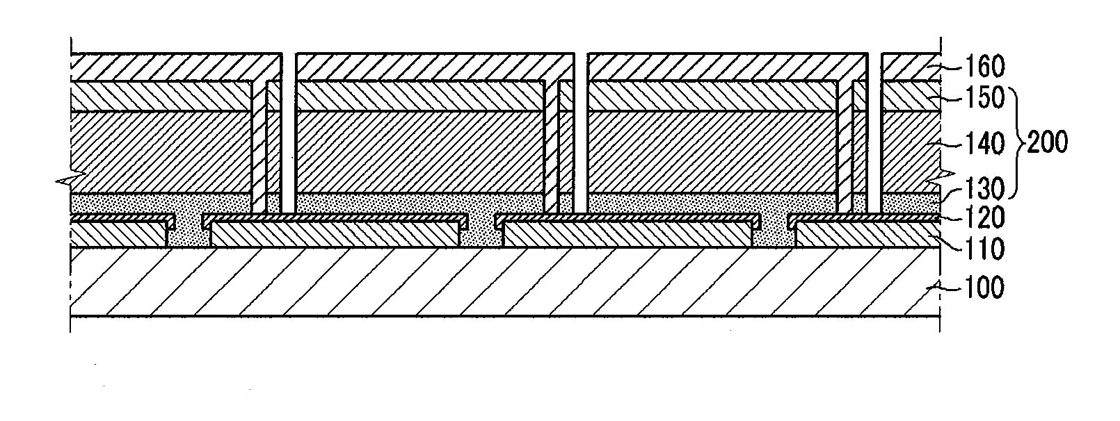
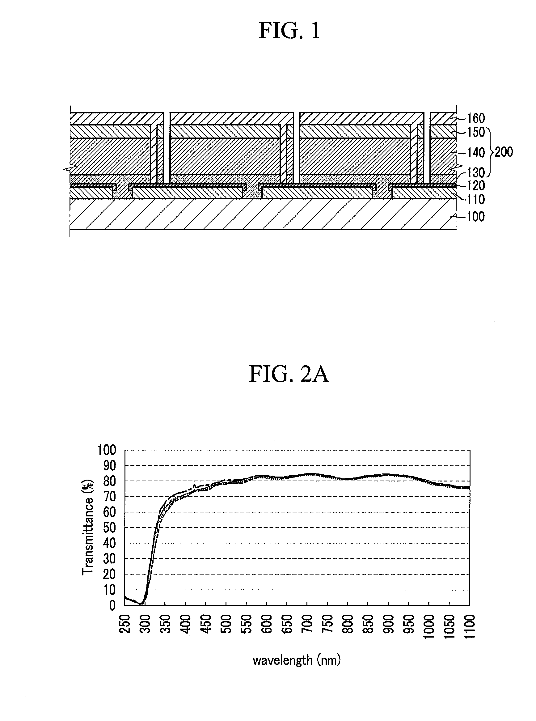
[0047]FIG. 1 is a cross-sectional view of a solar cell according to an embodiment of the present invention.

[0048]Referring to FIG. ...


PUM


Abstract

Photovoltaic devices and methods of manufacturing the same are provided. In one example, a photovoltaic device includes: a substrate; a transparent conductive layer deposited on the substrate; a semiconductor layer provided with a P layer, an I layer, and a N layer sequentially deposited on the transparent conductive layer; and a rear electrode deposited on the N layer of the semiconductor layer, wherein the P layer is a P-type oxide semiconductor.

Description

CROSS-REFERENCE TO RELATED APPLICATION[0001]This application claims priority to and the benefit of Korean Patent Application No. 10-2008-0057797 filed in the Korean Intellectual Property Office on Jun. 19, 2008, the entire contents of which are incorporated herein by reference.BACKGROUND OF THE INVENTION[0002](a) Field of the Invention[0003]The present invention relates to photovoltaic devices using an oxide semiconductor of a P type.[0004](b) Description of the Related Art[0005]A photovoltaic device converts light energy into electric energy. There are various kinds of photovoltaic devices according to the type of metal used, and one among them is a solar cell. A solar cell that converts the solar light energy into electric energy generates electricity by using two kinds of semiconductors that are referred to as a P-type semiconductor and a N-type semiconductor.[0006]The solar cells are largely categorized as a crystalline silicon solar cell that is used in most commercial products...

Claims


Application Information

Patent Timeline
Patent Type & Authority Applications(United States)
IPC IPC(8): H01L31/105H01L31/18H01L31/075
CPCY02E10/548H01L31/075Y02E10/549Y02P70/50H01L21/02592H01L21/041H01L21/32055H10K30/82H10K2102/351
Inventor LEE, CZANG-HOSHIN, MYUNG-HUNJUNG, SEUNG-JAESEO, JOON-YOUNGOH, MIN-SEOKLEE, BYOUNG-KYUKANG, KU-HYUNLIM, MI-HWA
Owner SAMSUNG SDI CO LTD
Why Eureka
Try Eureka