Semiconductor device and manufacturing method thereof

Active Publication Date: 2009-12-24
SANKEN ELECTRIC CO LTD
View PDF2 Cites 16 Cited by
  • Summary
  • Abstract
  • Description
  • Claims
  • Application Information

AI Technical Summary

Benefits of technology

[0010]The present invention attempts to resolve the above stated problems. Therefore, the present invention proposes a semiconductor device and a manufacturing method there

Problems solved by technology

The semiconductor wafer used in this type of IGBT is expensive due to the long time required for growth of the epitaxial layers and the cost of this semiconductor wafer significantly increases the manufacturing costs of the IGBT.
For example, because a semiconductor wafer is thinned by performing a back-grind process until the thickness of an n− type semiconductor layer (epitaxial layer) is reached, manu

Method used


Image

  • Semiconductor device and manufacturing method thereof
  • Semiconductor device and manufacturing method thereof
  • Semiconductor device and manufacturing method thereof

Examples


Example

First Embodiment

[0028]The first embodiment of the present invention explains an example in which the present invention is applied to an output type semiconductor device and manufacturing thereof comprised of an IGBT having a planar structure.

[Device Structure of a Semiconductor Device (IGBT)]

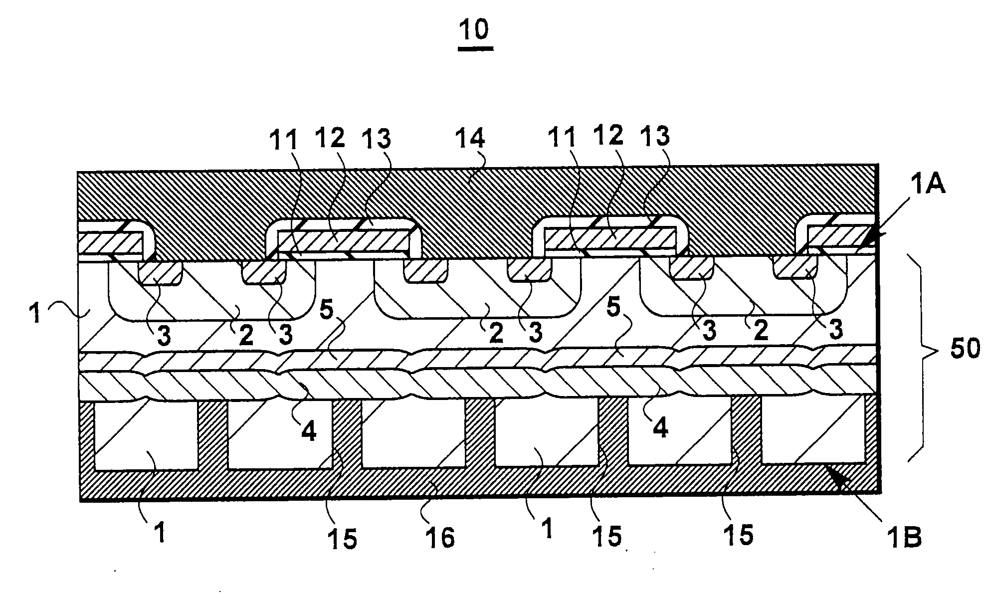
[0029]As is shown in FIG. 1, a semiconductor device (semiconductor chip) 10 related to the first embodiment is an IGBT and is arranged with a semiconductor substrate 50 which includes a first conductive first semiconductor region 1, arranged on one main surface 1A of the substrate 50, a plurality of second conductive second semiconductor regions 2 which are opposite to the first conductive type and are arranged at specific intervals on the one main surface 1A of the first semiconductor region 1, a plurality of first conductive third semiconductor regions 3 arranged separately on a main surface (the same main surface as the one main surface 1A) of the second semiconductor region 2, a gate electro...

Example

Second Embodiment

[0059]The second embodiment of the present invention explains an example in which a cross sectional structure of the fourth semiconductor region 4 arranged at the center part of the thickness direction of the first semiconductor region 1 at the bottom surface of the hole 15 in the semiconductor device 10 related to the first embodiment stated above is changed.

[Structure of the Semiconductor Device]

[0060]As is shown in FIG. 6, although the semiconductor device 10 related to the second embodiment is basically the same as the semiconductor 10 in which an IGBT is formed having a planar structure related to the first embodiment stated above, a second conductive fourth semiconductor region 4 is arranged along the bottom surface and side wall of the hole 15 of the first semiconductor region 1. The thickness of the fourth semiconductor region 4 is almost equal in both the bottom surface and side wall of the hole 15. Here, the hole 15 may be have a stripe shape or a dot shap...

Example

Third Embodiment

[0063]The third embodiment of the present invention explains an example in which the semiconductor device 10 related to the first embodiment stated above is replaced with a semiconductor device comprised from an IGBT having a trench gate structure.

[Structure of the Semiconductor Device]

[0064]As is shown in FIG. 8, the semiconductor device 10 related to the third embodiment is an IGBT which has a trench gate structure. That is, in the semiconductor device 10, a trench 17 is further arranged between adjacent second semiconductor regions 2 on one main surface 1A of the semiconductor substrate 50, a gate insulation film 11 is arranged along the bottom surface and side wall of the trench 17 and a gate electrode 12 buried within the trench 17 is arranged above this insulation film 11.

[0065]As was explained above, in the semiconductor device 10 related to the third embodiment, it is possible to demonstrate the same operational effects as those obtained by the semiconductor ...


PUM


Abstract

A manufacturing method of a semiconductor device 10 includes forming a plurality of second conductive second semiconductor regions at specific intervals on one main surface of a first conductive first semiconductor region, the plurality of second conductive second semiconductor regions being opposite to the first conductive first semiconductor region, forming a plurality of the first conductive third semiconductor regions on a main surface of the second semiconductor region, the plurality of the first conductive third regions being separated from each other, forming a plurality of holes at specific intervals on an another main surface which faces the one main surface of the first semiconductor region, the plurality of holes being separated from each other, forming a pair of adjacent second conductive fourth semiconductor regions which are alternately connected at a bottom part of the hole within the first semiconductor region, and burying an electrode within the hole.

Description

CROSS REFERENCE TO RELATED APPLICATION[0001]This application is based upon and claims the benefit of priority from the prior Japanese Patent Application No. 2008-163.250 filed on Jun. 23, 2008, the entire contents of which is incorporated herein by reference.BACKGROUND OF THE INVENTION[0002]1. Field of the Invention[0003]This invention relates to a semiconductor device and a method of manufacturing the same, and more particularly relates to a semiconductor device which operates as a switching device which can control a large current at high speeds, and a method of manufacturing such a semiconductor device.[0004]2. Description of the Related Art[0005]An IGBT (Insulated Gate Bipolar Transistor) is a semiconductor device which can control a large current at high speeds. In the manufacturing process of this IGBT, a semiconductor wafer in which two epitaxial layers of n+ type semiconductor layer (buffer layer) and an n− type semiconductor layer is made to grow on generally p type semicon...

Claims


Application Information

Patent Timeline
IPC IPC(8): H01L29/732H01L21/331
CPCH01L29/0653H01L29/7395H01L29/66333
Inventor IWABUCHI, AKIOKANEKO, SHUICHI
Owner SANKEN ELECTRIC CO LTD
Why Eureka
Try Eureka