Integrated trench Mosfet and Schottky Rectifier with trench contact structure

a technology of trench contact structure and mosfet, which is applied in the direction of diodes, semiconductor devices, electrical apparatus, etc., can solve the problems of needing additional fabrication costs, and achieve the effects of low reverse leakage current, low specific resistance, and low v

Inactive Publication Date: 2009-12-24
FORCE MOS TECH CO LTD
View PDF6 Cites 48 Cited by
  • Summary
  • Abstract
  • Description
  • Claims
  • Application Information

AI Technical Summary

Benefits of technology

[0012]One aspect of the present invention is that, the planar contact for both the MOSFET devices and Schottky barrier rectifier devices are replaced by the trench Schottky structure. By using this structure, the devices are able to be shrunk to achieve low specific on-resistance for trench MOSFET and, at the same time, achieve low Vf and low reverse leakage current for trench Schottky rectifier by applying a double epitaxial layer in a preferred embodiment.
[0013]Another aspect of the present invention is that, there's no need to use additional mask to open the anode of Schottky rectifier in fabricating process according to this invention, therefore cost saving is achieved.
[0015]Briefly, in another preferred embodiment, the structure disclosed is the same as structure mentioned in the first embodiment expect that the oxide at the bottom of trench gates is thicker than that of the first embodiment to further reduce the gate charge for power saving.
[0017]Briefly, in another preferred embodiment, the structure disclosed is the same as structure mentioned in the third embodiment except that the oxide at the bottom of trench gates is thicker than that of the third embodiment to further reduce the gate charge for power saving.

Problems solved by technology

On the other hand, this planar structure will lead to a device shrinkage limitation since the contacts occupy large area, resulting in high specific on-resistance according to the length dependence of resistance.
Another disadvantage of the structures mentioned in prior arts is that, during the fabricating process, additional P+ mask or contact mask for opening of Schottky rectifier anode contact is required, and therefore need additional fabrication cost.

Method used


Image

  • Integrated trench Mosfet and Schottky Rectifier with trench contact structure
  • Integrated trench Mosfet and Schottky Rectifier with trench contact structure
  • Integrated trench Mosfet and Schottky Rectifier with trench contact structure

Examples


Embodiment Construction

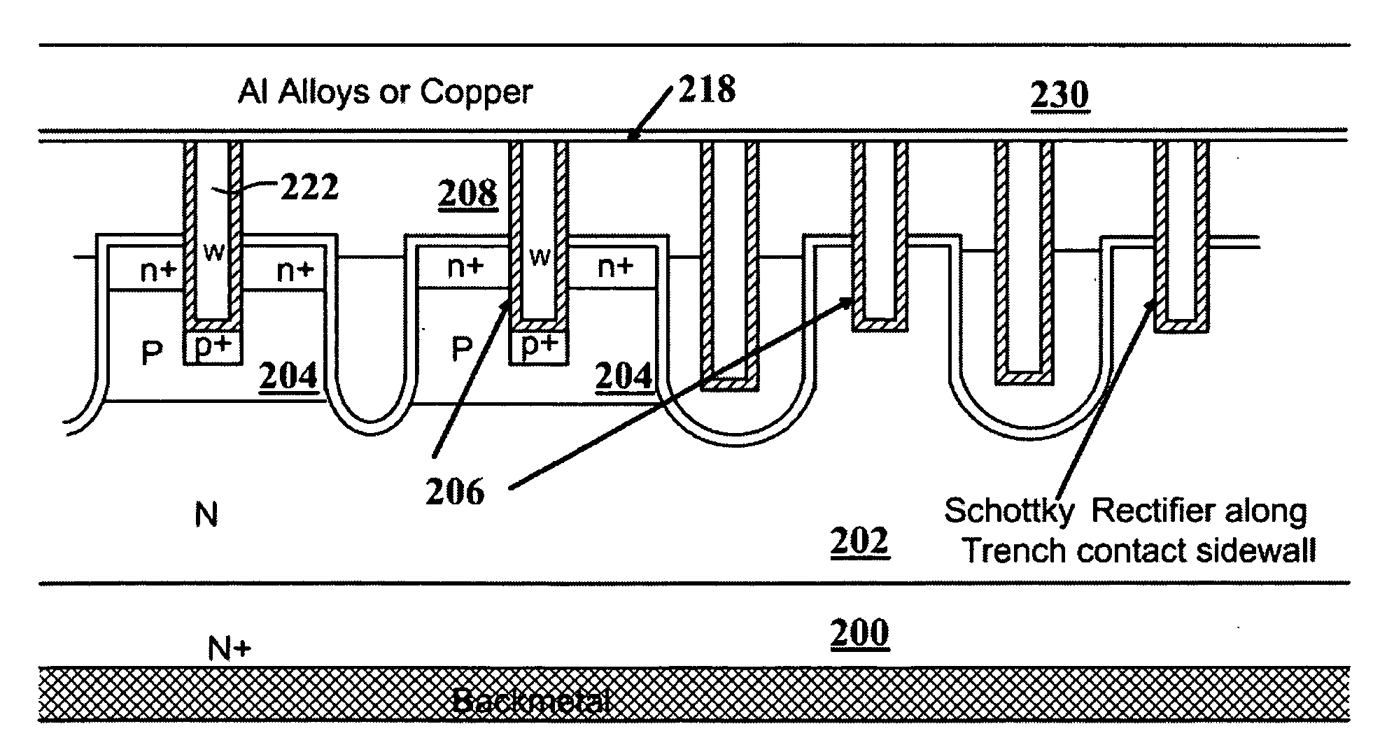
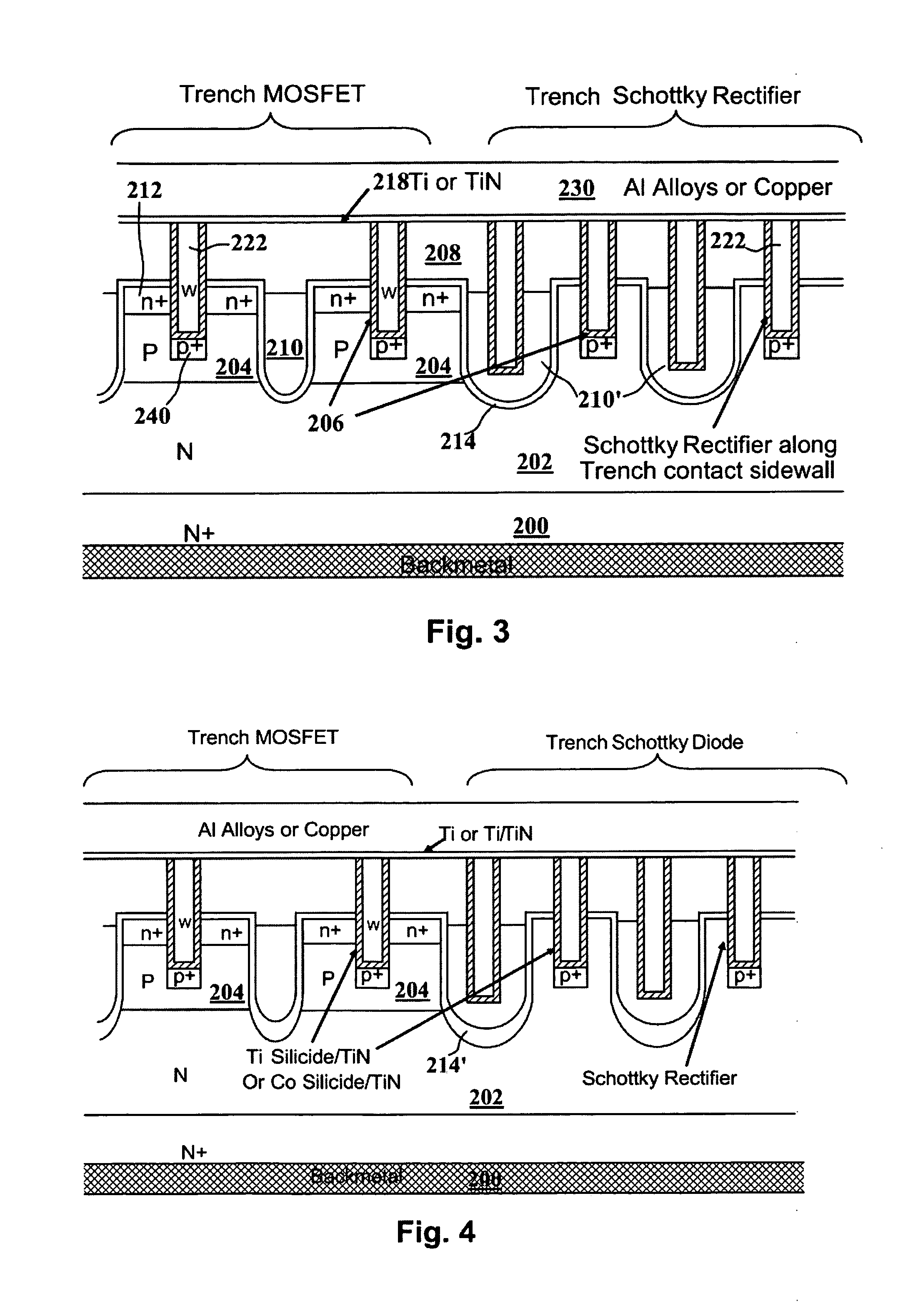
[0035]Please refer to FIG. 3 for a preferred embodiment of this invention where an integrated MOSFET device and Schottky barrier rectifier device is formed on a heavily N+ doped substrate 200 coated with back metal on rear side as drain, onto which formed an N epitaxial layer 202. The power MOS element further includes a plurality of trenched gates 210 and 210′ with a gate insulation layer 214 formed over the walls of the trenches. A body region 204 that is doped with a dopant of second conductivity type, e.g., P-type dopant, extends between the trenched gates expect between those used to form trench Schottky rectifier, and among all trenches, the trenches 210′ in Schottky barrier recitifer are wider than those in trench MOSFET. Doped poly is deposited as the gate material with a layer of gate oxide along the sidewall of trenches. Trench contacts are penetrating through source region 212 and into the body region 204 with an area of P+ doped area 240 at the bottom of each trench to r...


PUM


Abstract

A trench MOSFET in parallel with trench Schottky barrier rectifier is formed on a single substrate. The present invention solves the constrains brought by planar contact of Schottky, for example, the large area occupied by planar structure. As the size of present device is getting smaller and smaller, the trench Schottky structure of this invention is able to be shrink and, at the same time, to achieve low specific on-resistance. By applying a double epitaxial layer in trench Schottky barrier rectifier, the device performance is enhanced for lower Vf and lower reverse leakage current Ir is achieved.

Description

BACKGROUND OF THE INVENTION[0001]1. Field of the Invention[0002]This invention relates generally to integrated circuits comprising power MOSFETs in parallel with Schottky rectifiers. More particularly, this invention relates to a novel and improved structure and improved process of fabricating an integrated trench MOSFET and Schottky rectifier with trench contact structure upon a single substrate, which structure has improved performance with low specific on-resistance for Trench MOSFET and low Vf and reverse leakage current Ir for Trench Schottky rectifier, as well as low fabricating cost.[0003]2. The Prior Arts[0004]The Shottky barrier rectifiers have been used in DC-DC converters. In parallel with the parasitic PN body diode, the Schottky barrier rectifier acts as clamping diode to prevent the body diode from turning on for the reason of higher speed and efficiency, so the recent interests have been focus on the technology to integrate the MOSFET and the Schottky barrier rectifie...

Claims


Application Information

Patent Timeline
Patent Type & Authority Applications(United States)
IPC IPC(8): H01L27/105
CPCH01L27/0629H01L29/407H01L29/41766H01L29/42368H01L29/456H01L29/8725H01L29/66727H01L29/66734H01L29/7806H01L29/7813H01L29/47
Inventor HSIEH, FU-YUAN
Owner FORCE MOS TECH CO LTD
Why Eureka
Try Eureka