Maskless Doping Technique for Solar Cells

Inactive Publication Date: 2009-12-24
VARIAN SEMICON EQUIP ASSOC INC
View PDF16 Cites 40 Cited by
  • Summary
  • Abstract
  • Description
  • Claims
  • Application Information

AI Technical Summary

Benefits of technology

[0013]A improved, lower cost method of producing solar cells utilizing selective emitter design is disclosed. The contact regions are created on the substrate without the use of lithography or masks. The method utilizes ion implantation technology, and the relatively low accuracy requirements of the contact regions to reduce the process steps needed to produce a solar cell. In some embodiments, the current of the ion b

Problems solved by technology

The method utilizes ion implantation technology, and the relatively low accuracy require

Method used


Image

  • Maskless Doping Technique for Solar Cells
  • Maskless Doping Technique for Solar Cells
  • Maskless Doping Technique for Solar Cells

Examples


Embodiment Construction

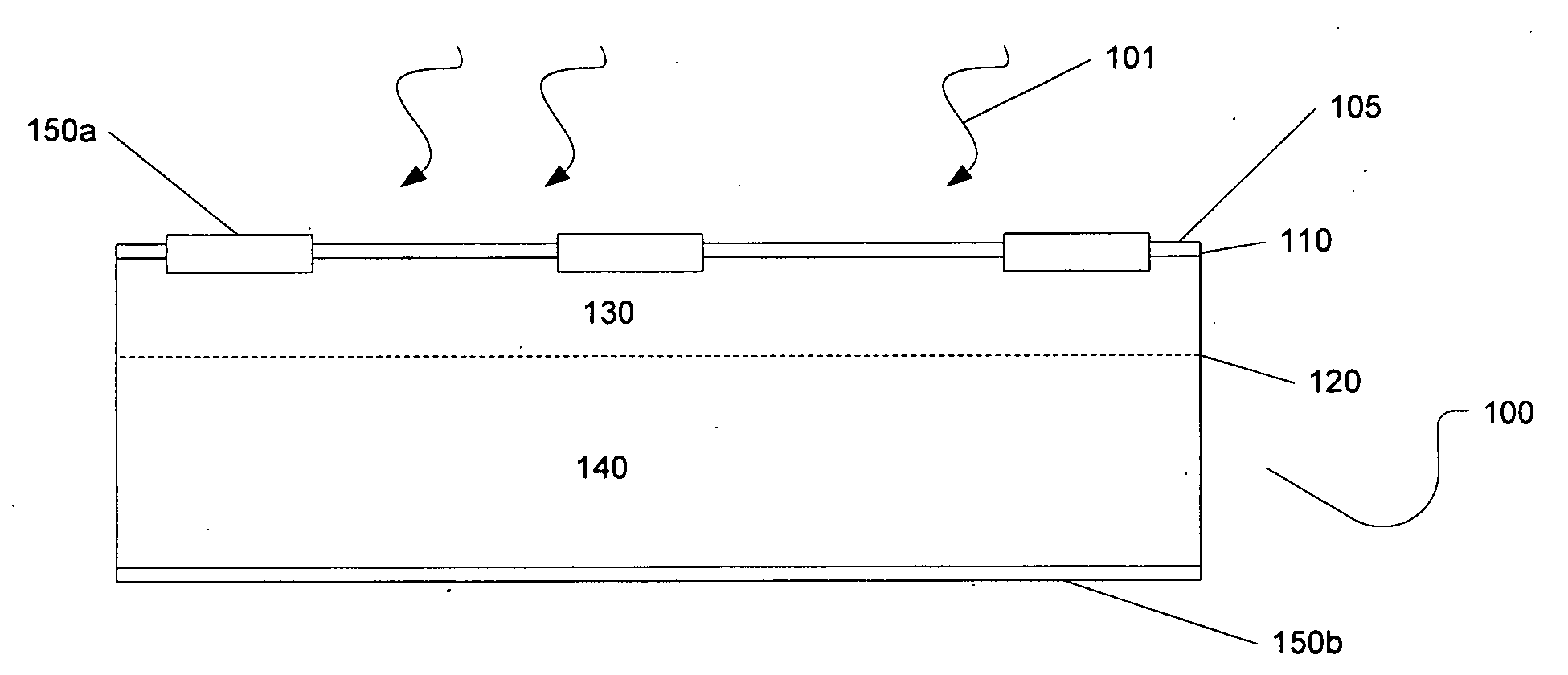
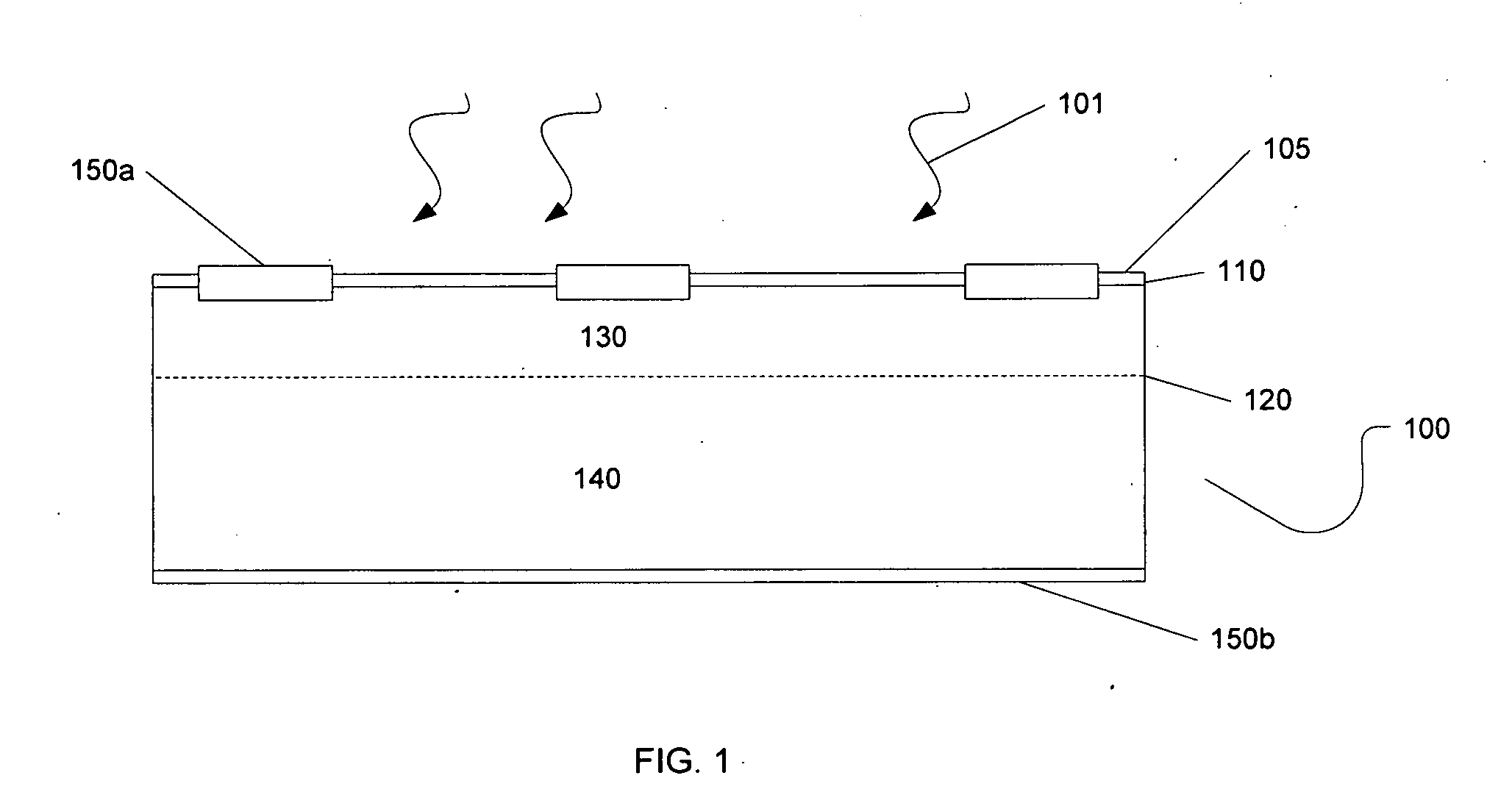
[0030]As described above, solar cells utilizing selective emitter design are most advantageous, however the manufacturing process needed to create such cells can be cost prohibitive. By understanding the relative accuracy and requirements of the solar cell, it is possible to manufacture solar cells having a selective emitter design without the costly lithography and masking process steps.

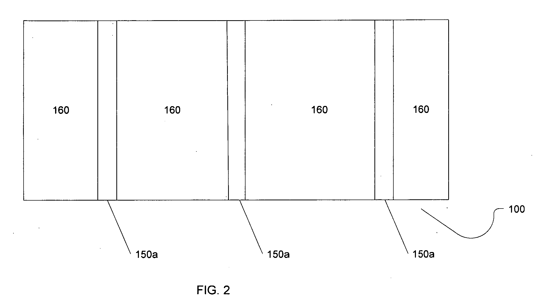
[0031]FIG. 4 shows a top view of the solar cell manufactured using the methods of the present disclosure. The solar cell is formed on a semiconductor substrate 100. The substrate can be any convenient size, including but not limited to circular, rectangular, or square. Although not a requirement, it is preferable that the width of the substrate 100 be less than the width of the ion beam used to implant ions in the substrate 100. However, no such limitation exists with respect to the orthogonal direction of the substrate. In other words, a substrate 100 can be arbitrarily long, and can be in the shap...


PUM


Abstract

A improved, lower cost method of producing solar cells utilizing selective emitter design is disclosed. The contact regions are created on the substrate without the use of lithography or masks. The method utilizes ion implantation technology, and the relatively low accuracy requirements of the contact regions to reduce the process steps needed to produce a solar cell. In some embodiments, the current of the ion beam is selectively modified to create the highly doped contact regions. In other embodiments, the ion beam is focused, either through the use of an aperture or via adjustments to the beam line components to create the necessary doping profile. In still other embodiments, the wafer scan rate is modified to create the desired ion implantation pattern.

Description

[0001]This application claims priority of U.S. Provisional Patent Application Ser. No. 61 / 074,278, filed Jun. 20, 2008, the disclosure of which is incorporated herein by reference.BACKGROUND OF THE INVENTION [0002]Solar cells are typically manufactured using the same processes used for other semiconductor devices, often using silicon as the substrate material. A semiconductor solar cell is a simple device having an in-built electric field that separates the charge carriers generated through the absorption of photons in the semiconductor material. This electric-field is typically created through the formation of a p-n junction (diode) which is created by differential doping of the semiconductor material. Doping a part of the semiconductor substrate (e.g. surface region) with impurities of opposite polarity forms a p-n junction that may be used as a photovoltaic device converting light into electricity.[0003]FIG. 1 shows a cross section of a representative substrate 100, comprising a ...

Claims


Application Information

Patent Timeline
IPC IPC(8): H01L21/00
CPCH01J37/3172H01J2237/31701H01L21/265Y02E10/547H01L31/068H01L31/1804H01L31/022425Y02P70/50
Inventor GUPTA, ATULBATEMAN, NICHOLASMURPHY, PAULRENAU, ANTHONYCARLSON, CHARLES
Owner VARIAN SEMICON EQUIP ASSOC INC
Why Eureka
Try Eureka