Wafer bonding apparatus

a wafer and interface technology, applied in the direction of mechanical control devices, instruments, process and machine control, etc., to achieve the effect of flatness of the wafer bonding interfa

Active Publication Date: 2009-12-24
NIKON CORP
View PDF4 Cites 25 Cited by
  • Summary
  • Abstract
  • Description
  • Claims
  • Application Information

AI Technical Summary

Benefits of technology

[0014]The heater unit includes plural heating modules, such that a deformation of the pressure profile control module can truly be transmitted to the top plate. A deformation of the top plate, caused by a variation in wafer thickness, is truly transmitted to the pressure profile control module. Therefore, the pressure profile control module can securely absorb the variation in wafer thickness.
[0015]Accordingly, the invention can provide the wafer bonding apparatus in which a shape of the pressurizing surface is changed to absorb a variation in wafer thickness such that the flatness of the wafer bonding interface may be improved while pressurizing and heating are performed.

Problems solved by technology

However, conventionally there has not been developed a wafer bonding apparatus in which a shape of a pressurizing surface is changed to absorb the variation in wafer thickness while the pressurizing and heating are performed in order to improve the flatness of the wafer bonding interface.

Method used


Image

  • Wafer bonding apparatus
  • Wafer bonding apparatus
  • Wafer bonding apparatus

Examples


Embodiment Construction

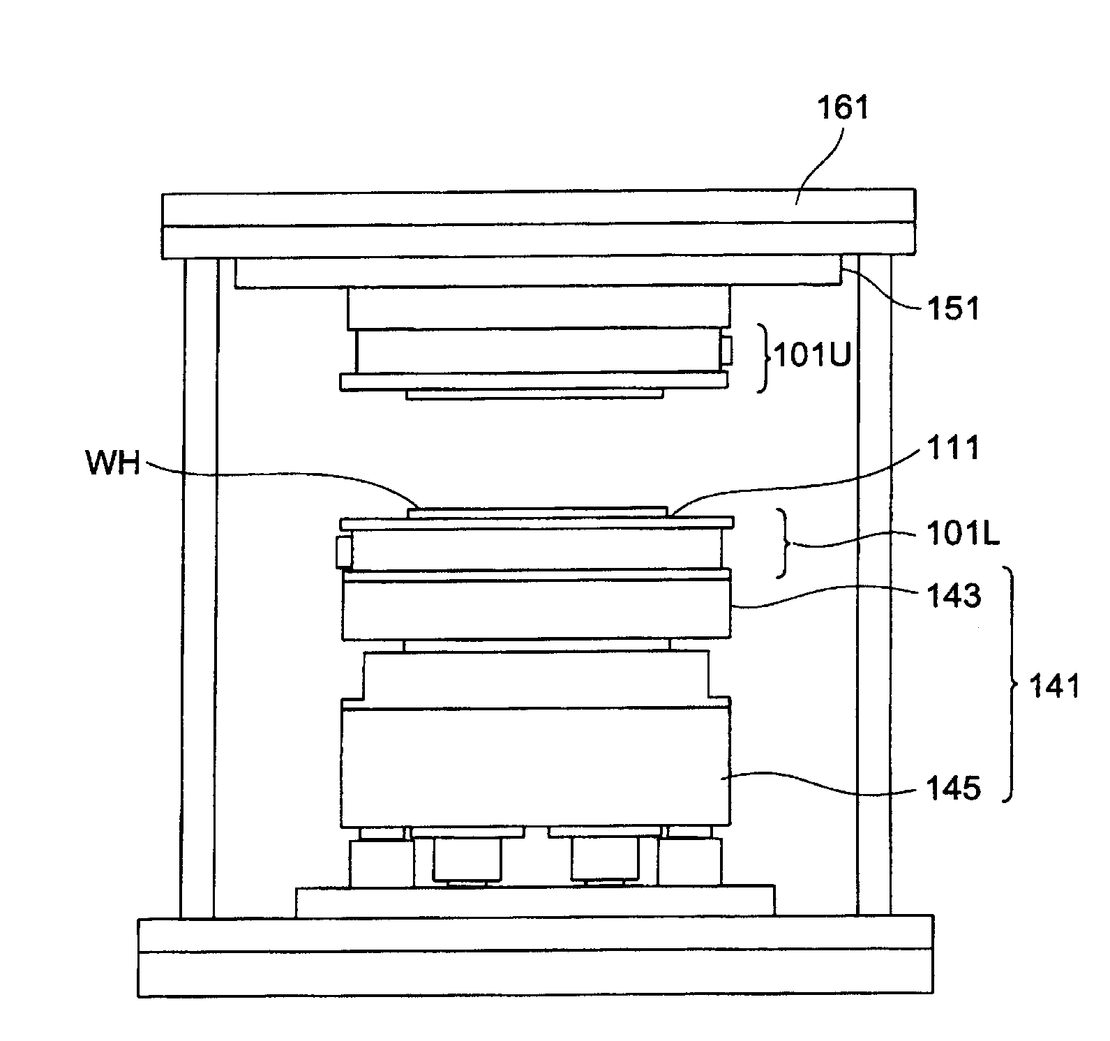
[0035]FIG. 1 is a view showing an entire configuration of a wafer bonding apparatus according to an embodiment of the invention.

[0036]The wafer bonding apparatus includes a pressurizing unit 141 and a base 151, which are attached to a vacuum chamber 161 while accommodated in the vacuum chamber 161. The pressurizing unit 141 includes a base 145 of the pressurizing unit and a lifting unit 143 of the pressurizing unit. A lower heater unit 101L is attached to the lifting unit 143 of the pressurizing unit. An upper heater unit 101U is attached to the base 151.

[0037]A wafer held by a wafer holder WH is disposed between the upper heater unit 101U and the lower heater unit 101L, and the wafer is pressurized and heated between the upper heater unit 101U and the lower heater unit 101L by lifting the lifting unit 143 of the pressurizing unit.

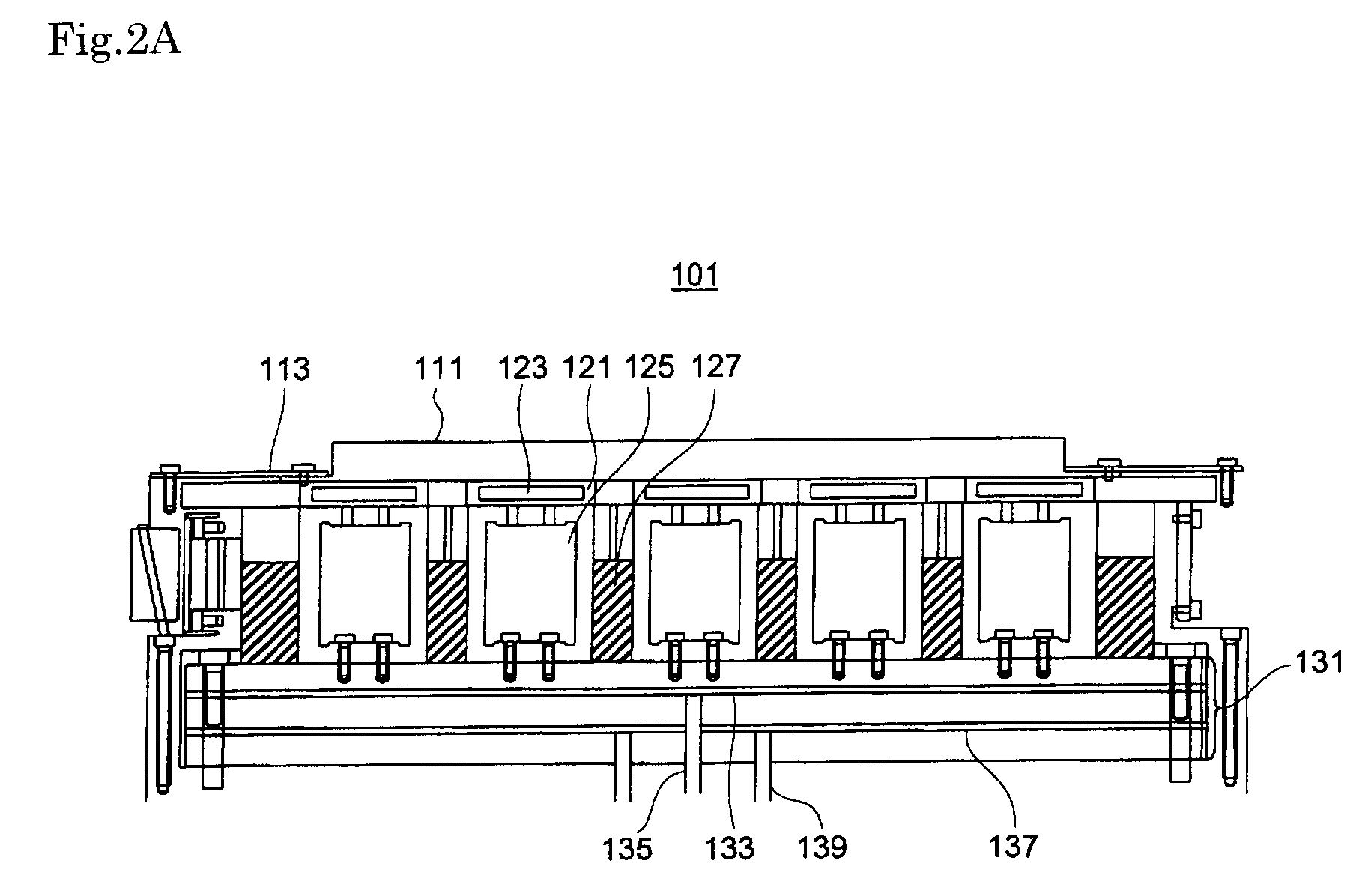
[0038]FIG. 2A is a view showing configurations of the upper heater unit 101U and lower heater unit 101L. Hereinafter the upper and lower heater units are ...


PUM

PropertyMeasurementUnit
thicknessaaaaaaaaaa
diameteraaaaaaaaaa
thicknessaaaaaaaaaa

Abstract

Provided is a wafer bonding apparatus which performs pressurization and heating and eliminates nonuniformity of wafer thickness by changing the shape of a pressurizing surface so that planarity of a wafer bonding surface is improved. The wafer bonding apparatus places a plurality of wafers to be bonded between an upper unit (101U) and a lower unit (101L), and bonds the wafers by applying pressure and heat by the upper unit and the lower unit. The wafer bonding apparatus is provided with a top plate (111), a pressure profile control module (131), and a heater section arranged between the top plate and the pressure profile control module for heating. Shape change generated on the surface of the pressure profile control module causes change of the surface of the top plate.

Description

TECHNICAL FIELD[0001]The present invention relates to a wafer bonding apparatus, in which plural wafers are placed such that one is put on another to bond electrodes, thereby producing a semiconductor integrated circuit. Particularly the invention relates to an apparatus, which bonds plural wafers while heating and pressurizing the wafers.BACKGROUND ART[0002]Recently a notebook personal computer, a portable telephone, and the like in which a semiconductor integrated circuit is used have a sophisticated function more and more. As a result, there is an increased need for higher density and higher functionality of the semiconductor integrated circuit.[0003]One of the method for realizing the high density and high functionality of the semiconductor integrated circuit is to laminate the wafer. In order to laminate the wafer, it is necessary that, after bonding electrodes are formed in wafer surfaces in which the circuit is already formed, the electrodes of two wafers or an already lamina...

Claims


Application Information

Patent Timeline
Patent Type & Authority Applications(United States)
IPC IPC(8): H01L21/30B32B37/02
CPCH01L21/2007H01L21/67092H01L24/80H01L2924/01029H01L2924/01033H01L2924/01046Y10T156/17H01L2924/14H01L2924/19043H01L2924/01005H01L2924/01006H01L2924/01047Y10T156/10H01L2924/01082H01L21/02
Inventor IZUMI, SHIGETO
Owner NIKON CORP
Why Eureka
Try Eureka