Method for manufacturing semiconductor device including metal gate electrode and semiconductor device

a manufacturing method and semiconductor technology, applied in the direction of semiconductor devices, electrical devices, transistors, etc., can solve the problems of inferior stability in manufacturing semiconductor devices, the threshold of transistors varies depending, etc., and achieve excellent manufacturing stability, excellent stability in manufacturing, and excellent stability

Inactive Publication Date: 2009-12-31
NEC ELECTRONICS CORP
View PDF0 Cites 8 Cited by
  • Summary
  • Abstract
  • Description
  • Claims
  • Application Information

AI Technical Summary

Benefits of technology

[0015]Accordingly, it is possible to prevent fluctuation of the thickness of the gate insulating film due to the embedding characteristics of the CVD system.
[0017]Since the first metal film mainly includes Ti or Ta, the first metal film can be easily removed, for example, by etching. Accordingly, the second dummy gate electrode as well as the gate electrode for the second MOS transistor can be stably formed.
[0019]For that reason, even when it is difficult to remove the second metal film by etching, the second metal film is removed by polishing. Thereby, the second metal film can be selectively removed with ease.
[0021]As mentioned above, a semiconductor device having excellent manufacture stability can be manufactured.
[0024]Since such a semiconductor device can be manufactured with the manufacturing method mentioned above, the semiconductor device has excellent stability in manufacture.
[0025]According to the exemplary aspect of the present invention, a semiconductor device having excellent manufacture stability and a method for manufacturing the semiconductor device are provided.

Problems solved by technology

Accordingly, there is a problem that a threshold of a transistor varies depending on the embedding characteristics of the CVD system.
For that reason, the threshold of the transistor cannot be set to a predetermined value, and therefore, the method has a problem of inferior stability in manufacturing the semiconductor device.

Method used


Image

  • Method for manufacturing semiconductor device including metal gate electrode and semiconductor device
  • Method for manufacturing semiconductor device including metal gate electrode and semiconductor device
  • Method for manufacturing semiconductor device including metal gate electrode and semiconductor device

Examples


first exemplary embodiment

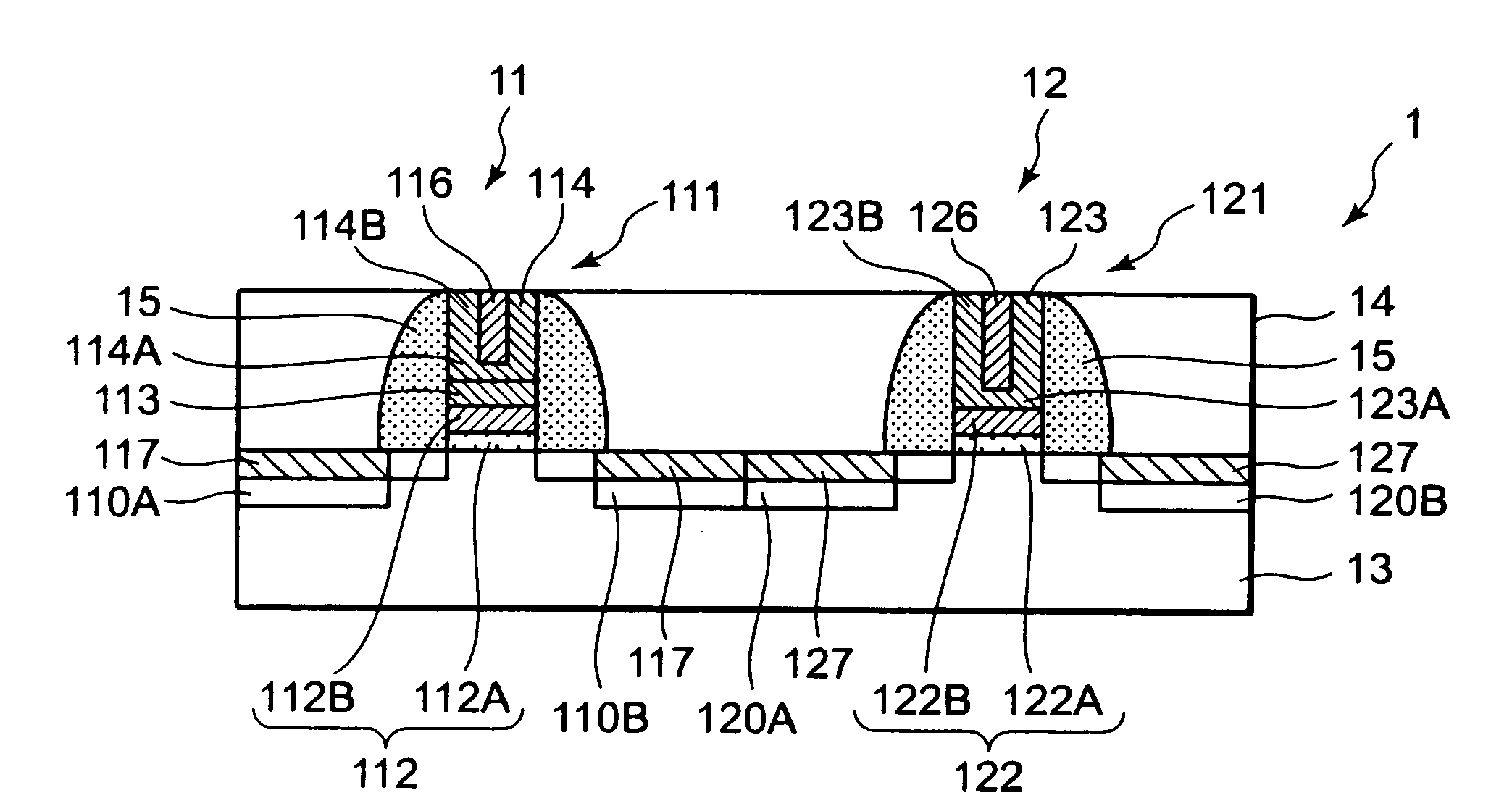
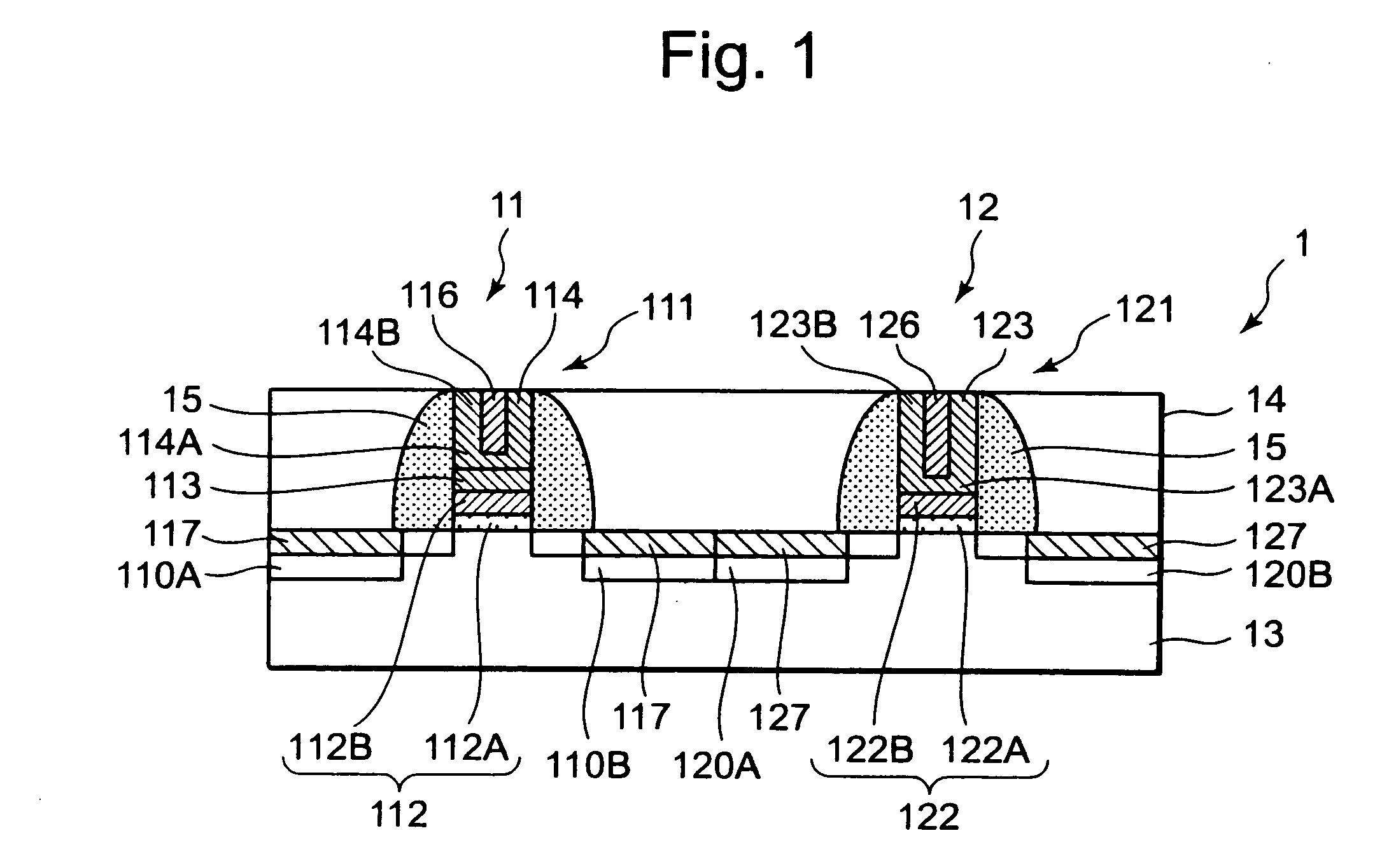
[0031]with reference to FIG. 1, description will be given on an outline of a semiconductor device 1 of the exemplary embodiment.

[0032]The semiconductor device 1 is a so-called CMOS device in which a p type MOS transistor (second MOS transistor) 11 and an n type MOS transistor (first MOS transistor) 12 are formed on a same semiconductor substrate 13. An insulating layer 14 is provided on the semiconductor substrate 13.

[0033]The n type MOS transistor 12 has a first gate electrode 121 formed within the insulating layer 14. The first gate electrode 121 includes an approximately plate-like gate insulating film 122 and a metal film 123 that has a covering part 123A for covering an approximately whole surface of the gate insulating film 122 and a peripheral wall part 123B provided upright on a periphery of the covering section 123A. The metal film 123 mainly includes one of metals of groups 6 to 8 in the periodic table and metals of groups 2 to 4 in the periodic table.

[0034]The p type MOS ...

second exemplary embodiment

[0074]FIG. 3 illustrates a semiconductor device according to a second exemplary embodiment of the present invention.

[0075]A semiconductor device 4 of the exemplary embodiment is a so-called CMOS device in which an n type MOS transistor (second MOS transistor) 41 and a p type MOS transistor (first MOS transistor) 42 are formed on a same semiconductor substrate 13.

[0076]The p type MOS transistor 42 has a first gate electrode 421 formed within an insulating layer 14. The first gate electrode 421 includes: an approximately plate-like gate insulating film 122 a metal film 423 having a covering part 423A for covering an approximately whole surface of the gate insulating film 122 and a peripheral wall part 423B provided upright on a periphery of the covering part 423A, the metal film 423 containing one of metals of groups 6 to 8 of the periodic table and metals of groups 2 to 4 of the periodic table; and a metal film 126. Here, the metal film 423 is a metal film mainly including Ru, for ex...


PUM


Abstract

A first metal film mainly including Ta is formed on a gate insulating film in a region excluding an n MOS transistor formation region and then a polysilicon film is formed to cover the gate insulating film and the first metal film. A first dummy electrode is formed by selectively removing the gate insulating film and the polysilicon film by etching, and a second dummy gate is formed by selectively removing the gate insulating film, the first metal film and the polysilicon film. An insulating layer is formed to embed the dummy gate electrodes and to expose an upper surface of the dummy gate electrodes. The polysilicon film of the dummy gate electrodes is removed to form recesses in the insulating layer, then a second metal film is formed within the recesses and on the insulating layer, and the second metal film is selectively polished.

Description

INCORPORATION BY REFERENCE[0001]The application is based upon and claims the benefit of priority from Japanese Patent Application No. 2008-165678 which was filed on Jun. 25, 2008, the disclosure of which is incorporated herein in its entirety by reference.BACKGROUND OF THE INVENTION[0002]1. Field of the Invention[0003]The present invention relates to a method for manufacturing a semiconductor device, and to a semiconductor device.[0004]2. Description of Related Art[0005]As a related art, semiconductor devices in which an n type MOSFET and a p type MOSFET are provided on the same semiconductor substrate have been used.[0006]In such a semiconductor device, a threshold voltage value needs to be set in accordance with each MOSFET to have a value suitable for the MOSFET. To meet the need, methods have been proposed in which a metal material having a work function suitable for a gate electrode of each MOSFET is selected.[0007]Japanese Patent Application Laid Open No. 2006-351580 discloses...

Claims


Application Information

Patent Timeline
Patent Type & Authority Applications(United States)
IPC IPC(8): H01L27/092H01L21/28
CPCH01L21/28088H01L21/823842H01L29/66545H01L29/513H01L29/665H01L29/4966
Inventor MATSUBARA, YOSHIHISA
Owner NEC ELECTRONICS CORP
Why Eureka
Try Eureka