Layered chip package and method of manufacturing same

a chip and layer technology, applied in the direction of electrical equipment, semiconductor devices, semiconductor/solid-state device details, etc., can solve the problems of increasing the cost of the layered chip package, affecting the high-speed operation of the circuit, and difficulty in reducing the distance between the electrodes, etc., to achieve the effect of short time, low cost and increased variety of electrical connections

Inactive Publication Date: 2009-12-31
HEADWAY TECH INC +1
View PDF3 Cites 34 Cited by
  • Summary
  • Abstract
  • Description
  • Claims
  • Application Information

AI Technical Summary

Benefits of technology

[0017]It is an object of the present invention to provide a layered chip package, a method of manufacturing the same, and an electronic component including a plurality of layered chip packages to allow mass-production of a layered chip package including a stack of a plurality of chips at low cost in a short period of time, and to increase the variety of electrical connection between a plurality of layered chip packages.
[0033]The layered chip package, its manufacturing method and the electronic component of the present invention make it possible to mass-produce the layered chip package at low cost in a short period of time, and to increase the variety of electrical connection between a plurality of layered chip packages.
[0034]The electronic component of the present invention allows easy reworking (remaking) of the electronic component including a plurality of layer portions.

Problems solved by technology

The wire bonding method has a problem that it is difficult to reduce the distance between the electrodes so as to avoid contact between wires, and a problem that high resistances of the wires hamper a high-speed operation of a circuit.
Unfortunately, however, the through electrode method requires a large number of steps for forming the through electrodes in chips, and consequently increases the cost for the layered chip package.
Consequently, voids or keyholes are prone to occur in the through electrodes due to poor filling of the holes with metal, so that the reliability of wiring formed by the through electrodes tends to be reduced.
When the upper and lower chips are joined to each other at high temperatures, however, misalignment between the upper and lower chips can occur due to expansion and contraction of the chips, which often results in electrical connection failure between the upper and lower chips.
The through electrode method has a further problem that, if the plurality of chips stacked include one or more defective chips, it is difficult to replace the defective chip(s) with non-defective one(s).
This heating also melts solder between non-defective chips, and can thereby cause oxidation or flowing-out of the solder between the non-defective chips.
As a result, electrical connection failure can occur between the non-defective chips.
For this reason, according to the through electrode method, it is difficult to replace one or more defective chips, if included in the stack of a plurality of chips, with non-defective one(s).
This can result in a reduction in yield and an increase in cost for the layered chip package.
The manufacturing method disclosed in U.S. Pat. No. 5,953,588 involves a number of process steps and this raises the cost for the layered chip package.
This is also a factor that raises the cost for the layered chip package.
According to this multilayer module, however, it is impossible to increase the proportion of the area occupied by the electronic element in each active layer, and consequently it is difficult to achieve higher integration.
In this case, the plurality of electronic component packages and wiring for electrically connecting them to each other occupy a large area of the wiring board, and this makes it difficult to achieve miniaturization of a system including the plurality of electronic component packages and the wiring board.

Method used


Image

  • Layered chip package and method of manufacturing same
  • Layered chip package and method of manufacturing same
  • Layered chip package and method of manufacturing same

Examples


first embodiment

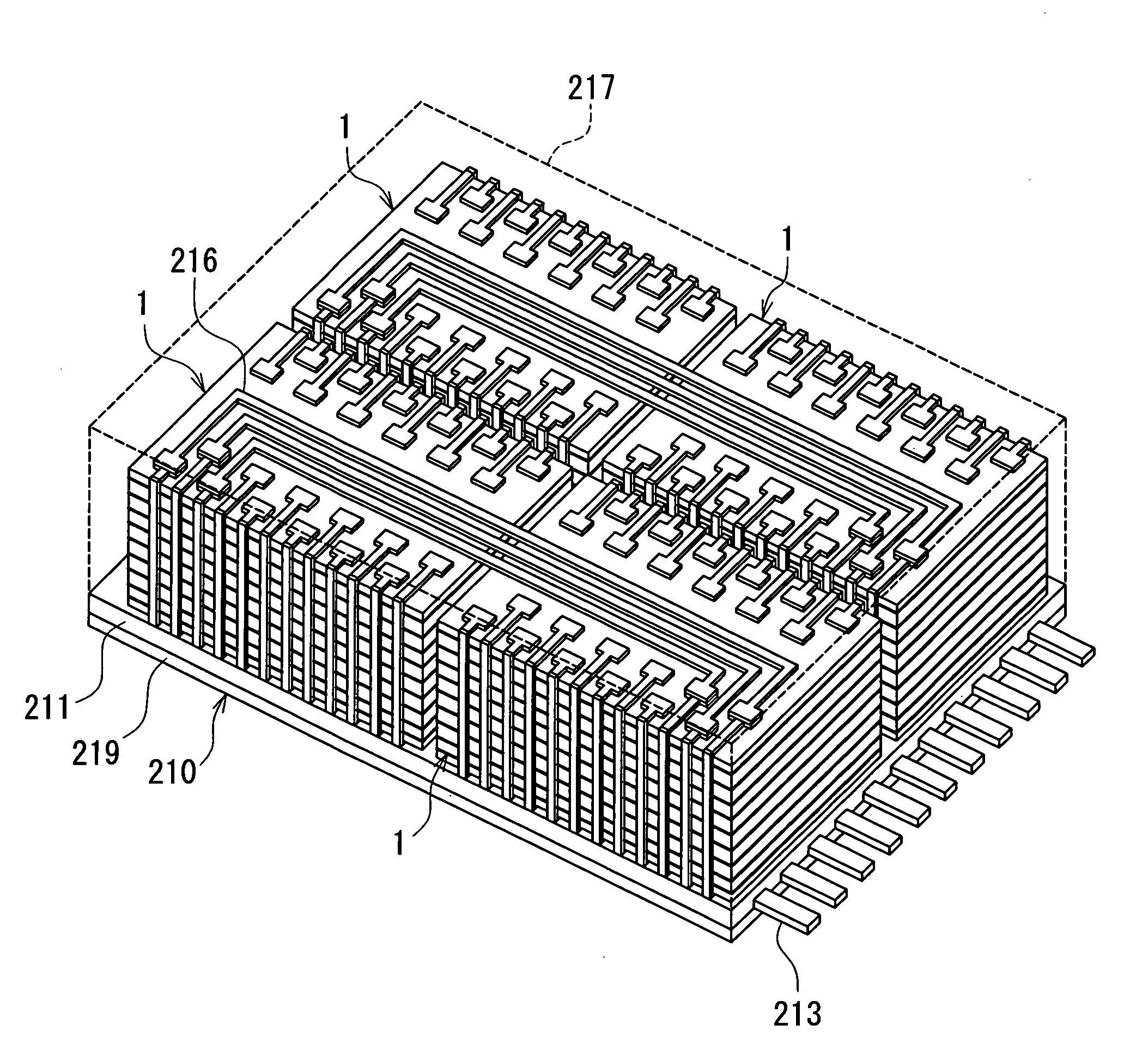
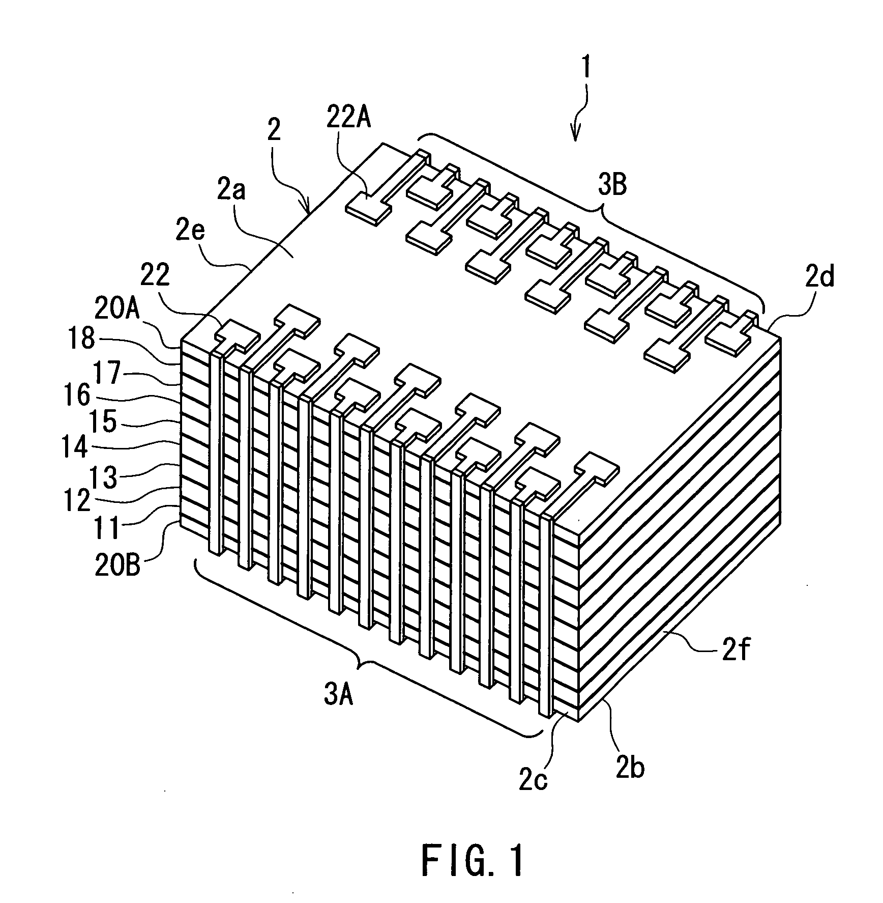
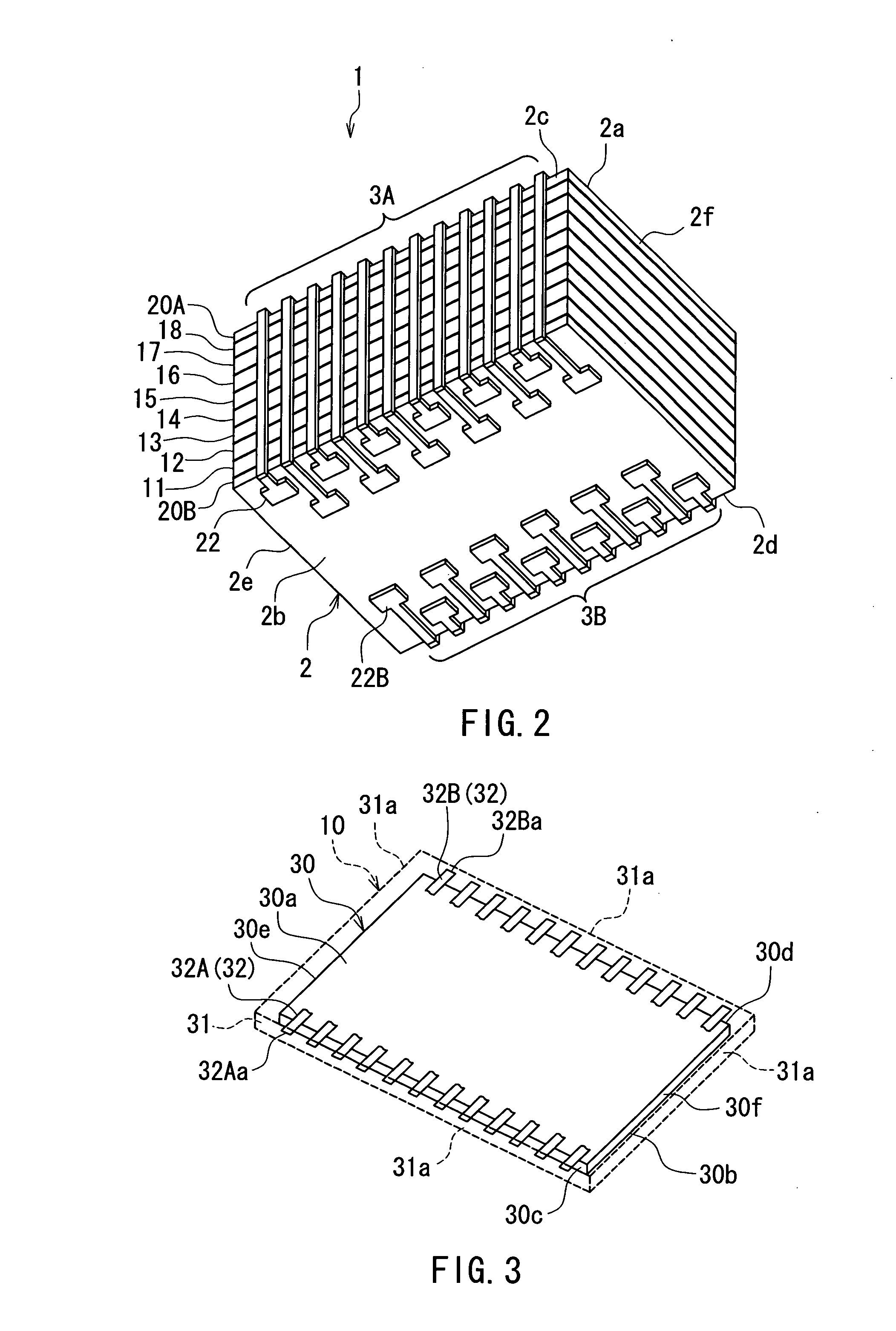
[0079]Embodiments of the present invention will now be described in detail with reference to the drawings. Reference is first made to FIG. 1 and FIG. 2 to describe the configuration of a layered chip package of a first embodiment of the invention. FIG. 1 is a perspective view of the layered chip package of the first embodiment. FIG. 2 is a perspective view of the layered chip package of FIG. 1 as seen from the bottom surface. As shown in FIG. 1 and FIG. 2, the layered chip package 1 of the first embodiment includes a main body 2 that is rectangular-solid-shaped. The main body 2 has a top surface 2a, a bottom surface 2b, a first side surface 2c and a second side surface 2d facing toward opposite directions, and a third side surface 2e and a fourth side surface 2f facing toward opposite directions.

[0080]The layered chip package 1 further includes wiring disposed on at least one of the side surfaces of the main body 2. In the example shown in FIG. 1 and FIG. 2, the layered chip package...

second embodiment

[0179]A second embodiment of the present invention will now be described. The appearance of the layered chip package 1 of the second embodiment is as shown in FIG. 1 and FIG. 2, as in the case of the first embodiment.

[0180]FIG. 42 is a perspective view of a layer portion 10 of the second embodiment. According to the second embodiment, the third side surface 30e and the fourth side surface 30f of the semiconductor chip 30 are respectively located at the third side surface 2e and the fourth side surface 2f of the main body 2. The first side surface 30c and the second side surface 30d of the semiconductor chip 30 respectively face toward the first side surface 2c and the second side surface 2d of the main body. In the second embodiment, of the four side surfaces of the semiconductor chip 30, the first side surface 30c and the second side surface 30d are covered with the insulating portion 31 whereas the third side surface 30e and the fourth side surface 30f are not covered with the ins...


PUM


Abstract

A layered chip package includes: a main body including a plurality of layer portions; wiring disposed on a side surface of the main body; a plurality of first terminals disposed on a top surface of the main body; and a plurality of second terminals disposed on a bottom surface of the main body. Each layer portion includes a semiconductor chip, an insulating portion covering at least one side surface of the semiconductor chip, and a plurality of electrodes connected to the semiconductor chip. Each electrode has an end face surrounded by the insulating portion and located at the side surface of the main body on which the wiring is disposed. The wiring is connected to the end faces of the plurality of electrodes of the plurality of layer portions, and to the plurality of first and second terminals.

Description

BACKGROUND OF THE INVENTION[0001]1. Field of the Invention[0002]The present invention relates to a layered chip package including a plurality of chips stacked, and to a method of manufacturing the same.[0003]2. Description of the Related Art[0004]In recent years, a reduction in weight and an improvement in performance have been demanded of mobile devices typified by cellular phones and notebook personal computers. Accordingly, there has been a demand for higher integration of electronic components for use in mobile devices. Higher integration of electronic components has been demanded also for achieving an increase in capacity of semiconductor memory.[0005]As an example of highly integrated electronic components, a system-in-package (hereinafter referred to as SiP), especially an SiP utilizing a three-dimensional packaging technology for stacking a plurality of chips, has attracting attention in recent years. In the present application, a package including a plurality of chips stack...

Claims


Application Information

Patent Timeline
Patent Type & Authority Applications(United States)
IPC IPC(8): H01L23/52H01L21/00
CPCH01L21/6835H01L23/544H01L2924/07802H01L24/24H01L24/82H01L24/92H01L24/95H01L25/0652H01L25/0657H01L25/50H01L2221/68359H01L2223/5442H01L2223/54426H01L2224/24145H01L2225/06524H01L2225/06527H01L2225/06551H01L2924/01015H01L2924/01029H01L2924/01075H01L2924/01078H01L2924/01082H01L2924/30105H01L2924/01006H01L2924/01033H01L2924/00H01L2924/181
Inventor SASAKI, YOSHITAKAITO, HIROYUKIHARADA, TATSUYAOKUZAWA, NOBUYUKISUEKI, SATORU
Owner HEADWAY TECH INC
Why Eureka
Try Eureka