Methods of Fabricating a BEOL Wiring Structure Containing an On-Chip Inductor and an On-Chip Capacitor

a technology of on-chip inductance and capacitor, which is applied in the direction of impedence network, inductance, and details of semiconductor/solid-state devices, can solve the problems of inefficient use of surface area by on-chip passive devices in the beol wiring structure, and achieve the effect of conserving the chip area required

Active Publication Date: 2009-12-31
AURIGA INNOVATIONS INC
View PDF11 Cites 19 Cited by
  • Summary
  • Abstract
  • Description
  • Claims
  • Application Information

AI Technical Summary

Benefits of technology

[0008]The vertically stacked arrangement or layout for the on-chip capacitor and the on-chip inductor in the BEOL wiring structure conserves the chip area required for these passive devices by providing a compact form factor. As a result, more area is available in the BEOL wiring structure for connections with the active devices carried on the chip. Because of the vertically stacked layout, the on-chip capacitor may also function as a Faraday shield so that a discrete Faraday shield may be omitted from the BEOL wiring structure.

Problems solved by technology

Despite their usefulness, on-chip passive devices tend to make rather inefficient use of the surface area in the BEOL wiring structure.

Method used


Image

  • Methods of Fabricating a BEOL Wiring Structure Containing an On-Chip Inductor and an On-Chip Capacitor
  • Methods of Fabricating a BEOL Wiring Structure Containing an On-Chip Inductor and an On-Chip Capacitor
  • Methods of Fabricating a BEOL Wiring Structure Containing an On-Chip Inductor and an On-Chip Capacitor

Examples


Embodiment Construction

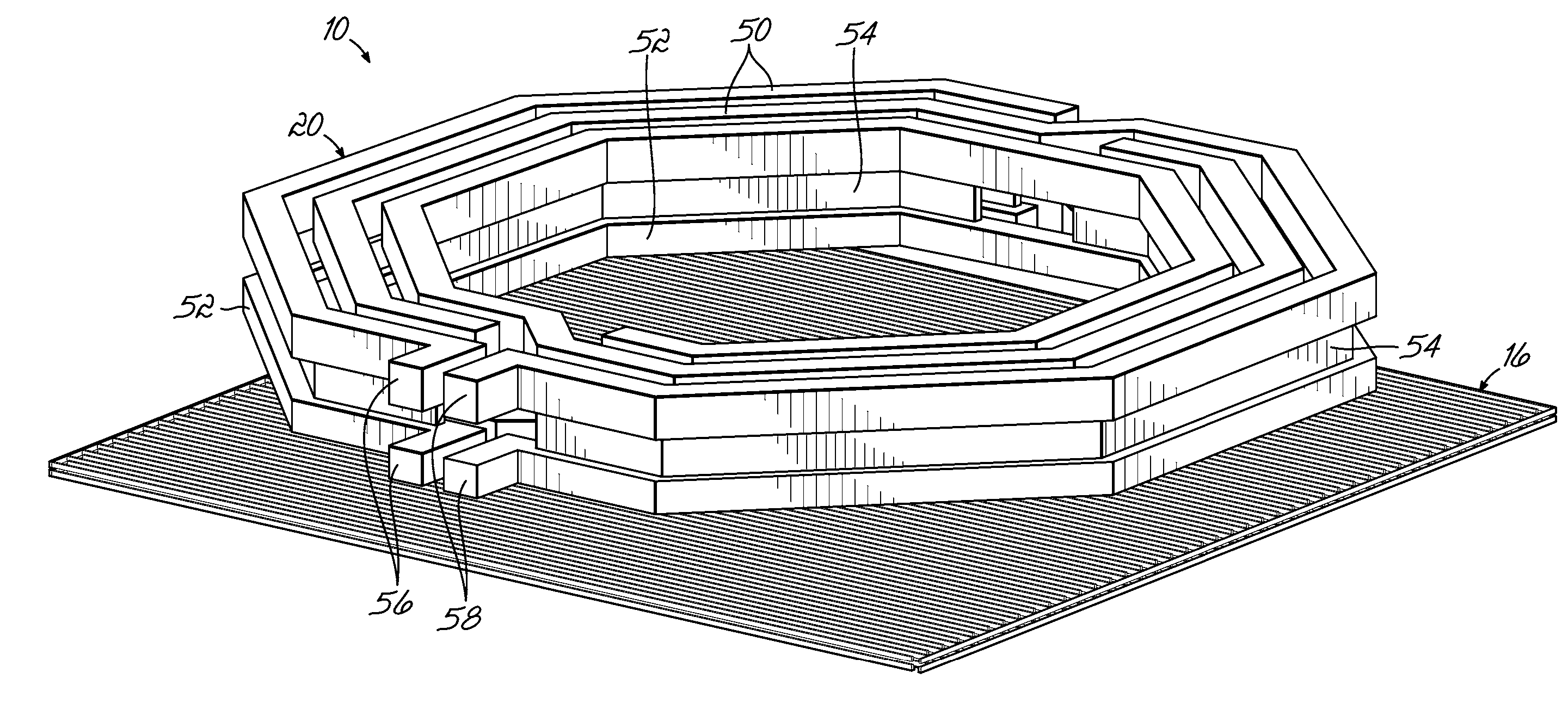
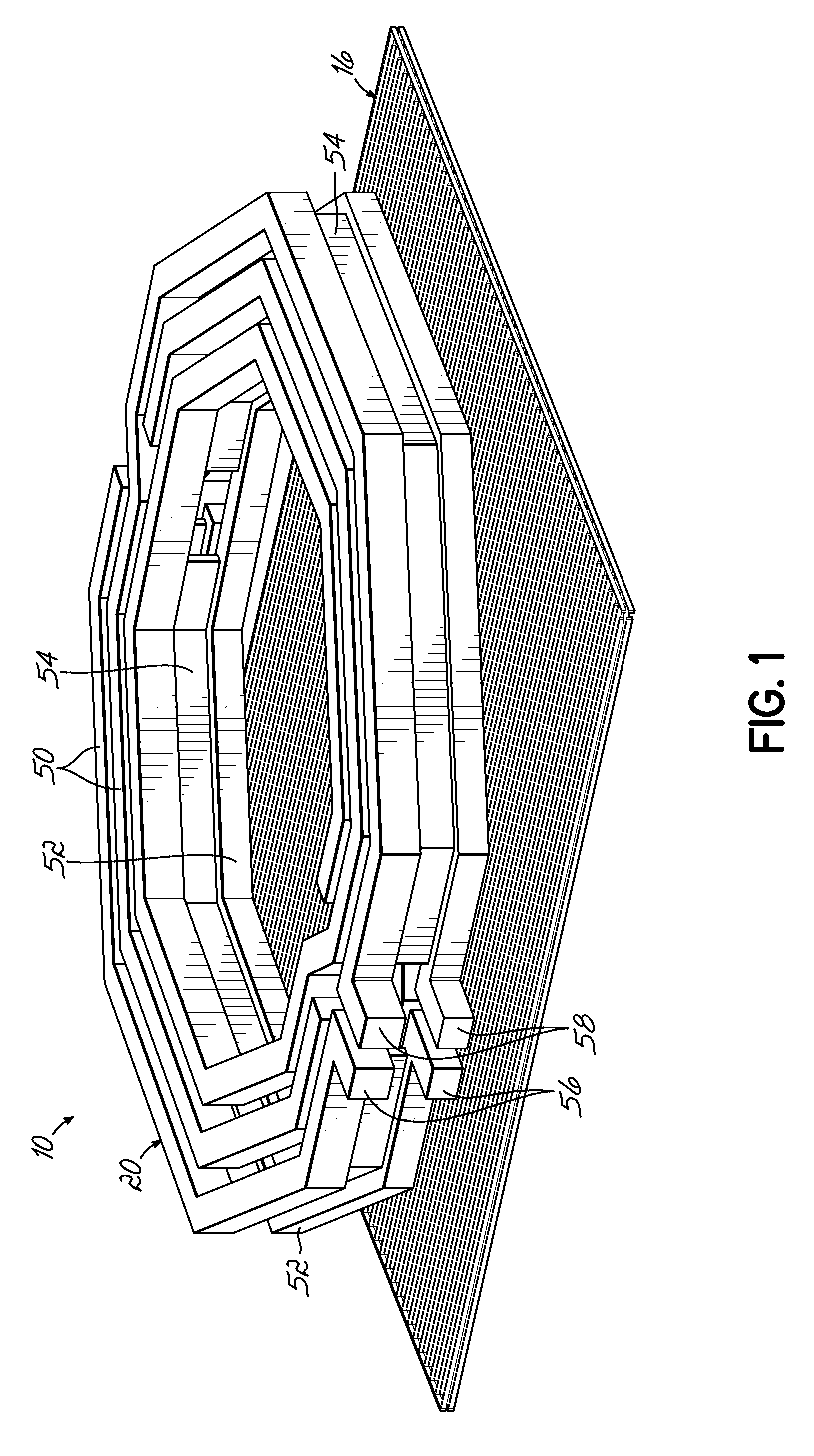
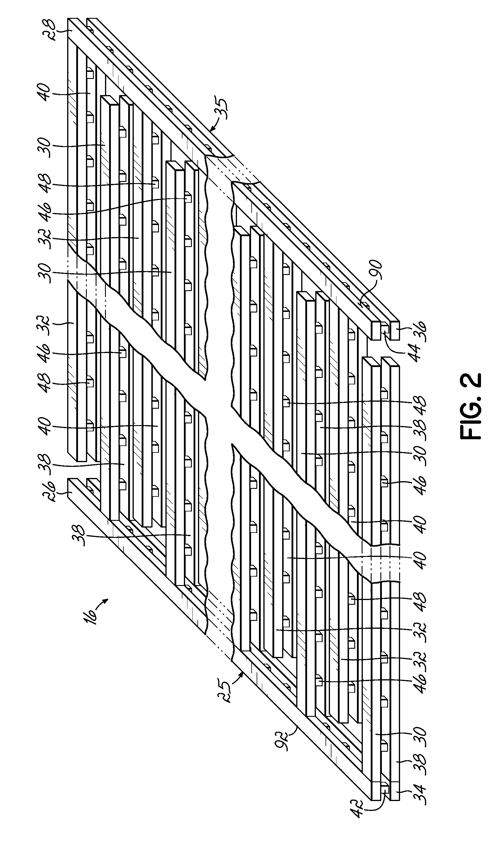
[0022]With reference to FIGS. 1, 2, 2A, 2B and in accordance with an embodiment of the invention, a back-end-of-line (BEOL) wiring structure, generally indicated by reference numeral 10, includes a dielectric layer 12 of a metallization level (Mx), a dielectric layer 14 of a metallization level (Mx−1) underlying the metallization level (Mx), an on-chip capacitor 16 embedded in the dielectric layers 12, 14, a dielectric layer 18 of an upper metallization level (Mx+1) overlying the metallization level (Mx), a dielectric layer 19 of an upper metallization level (Mx+2) overlying the metallization level (Mx−a), and an on-chip inductor 20 embedded in the dielectric layers 18, 19. Additional metallization levels (not shown) may exist below the metallization level (Mx−1), between metallization level (Mx) and metallization levels (Mx+1, Mx+2), and / or above the upper metallization levels (Mx+1, Mx+2). Conductive features in the different metallization levels of the BEOL wiring structure, such...


PUM


Abstract

Methods for fabricating a back-end-of-line (BEOL) wiring structure that includes an on-chip inductor and an on-chip capacitor, as well as methods for tuning and fabricating a resonator that includes the on-chip inductor and on-chip capacitor. The fabrication methods generally include forming the on-chip capacitor and on-chip inductor in different metallization levels of the BEOL wiring structure and laterally positioned to be substantially vertical alignment. The on-chip capacitor may serve as a Faraday shield for the on-chip inductor. Optionally, a Faraday shield may be fabricated either between the on-chip capacitor and the on-chip inductor, or between the on-chip capacitor and the substrate. The BEOL wiring structure may include at least one floating electrode capable of being selectively coupled with the directly-connected electrodes of the on-chip capacitor for tuning, during circuit operation, a resonance frequency of an LC resonator that further includes the on-chip inductor.

Description

CROSS-REFERENCE TO RELATED APPLICATIONS[0001]This application is related to application Ser. No. ______, filed as Attorney Docket No. BUR920080203US2 on even date herewith and entitled “BEOL WIRING STRUCTURES THAT INCLUDE AN ON-CHIP INDUCTOR AND AN ON-CHIP CAPACITOR, AND DESIGN STRUCTURES FOR A RADIOFREQUENCY INTEGRATED CIRCUIT”, which is hereby incorporated by reference herein in its entirety.FIELD OF THE INVENTION[0002]The invention relates generally to semiconductor device fabrication and, in particular, to methods for fabricating back-end-of-line wiring structures that include an on-chip inductor and an on-chip capacitor, as well as methods for tuning a resonator that includes the on-chip inductor and on-chip capacitor.BACKGROUND OF THE INVENTION[0003]Capacitors and inductors represent two types of on-chip passive devices commonly employed in many types of monolithic integrated circuits designed to operate at high frequencies, such as those found in wireless communication device...

Claims


Application Information

Patent Timeline
Patent Type & Authority Applications(United States)
IPC IPC(8): H03H7/00H01L21/02
CPCH01F2017/0046H01F2017/008H01F2021/125H01L23/5222H01L23/5227H01L27/0794H01L28/10H01L2924/0002H01L28/20H01L2924/3011H03H2001/0014H03H2001/0092H01L2924/00H01L23/5223H01L23/5225
Inventor DALEY, DOUGLAS M.ERTURK, METEGORDON, EDWARD J.
Owner AURIGA INNOVATIONS INC
Why Eureka
Try Eureka