

BEOL Wiring Structures That Include an On-Chip Inductor and an On-Chip Capacitor, and Design Structures for a Radiofrequency Integrated Circuit
a technology of on-chip capacitors and wiring structures, applied in the direction of multiple-port networks, pulse automatic control, transformer/react mounting/support/suspension, etc., can solve the problem that the surface area of the beol wiring structure is rather inefficient, and achieve the effect of conserving the chip area required
- Summary
- Abstract
- Description
- Claims
- Application Information
AI Technical Summary
Benefits of technology
Problems solved by technology
Method used
Image

Examples
Embodiment Construction
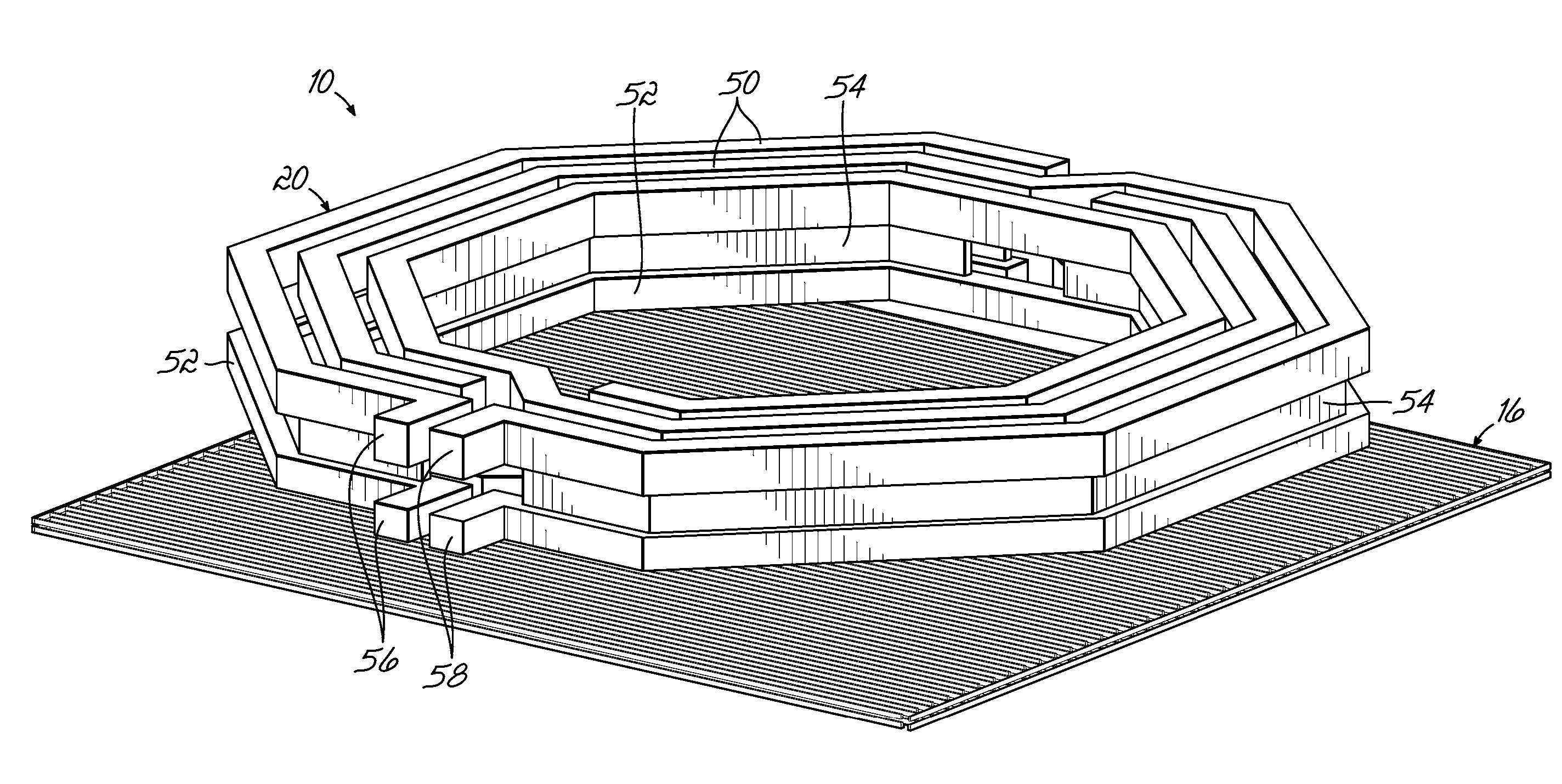
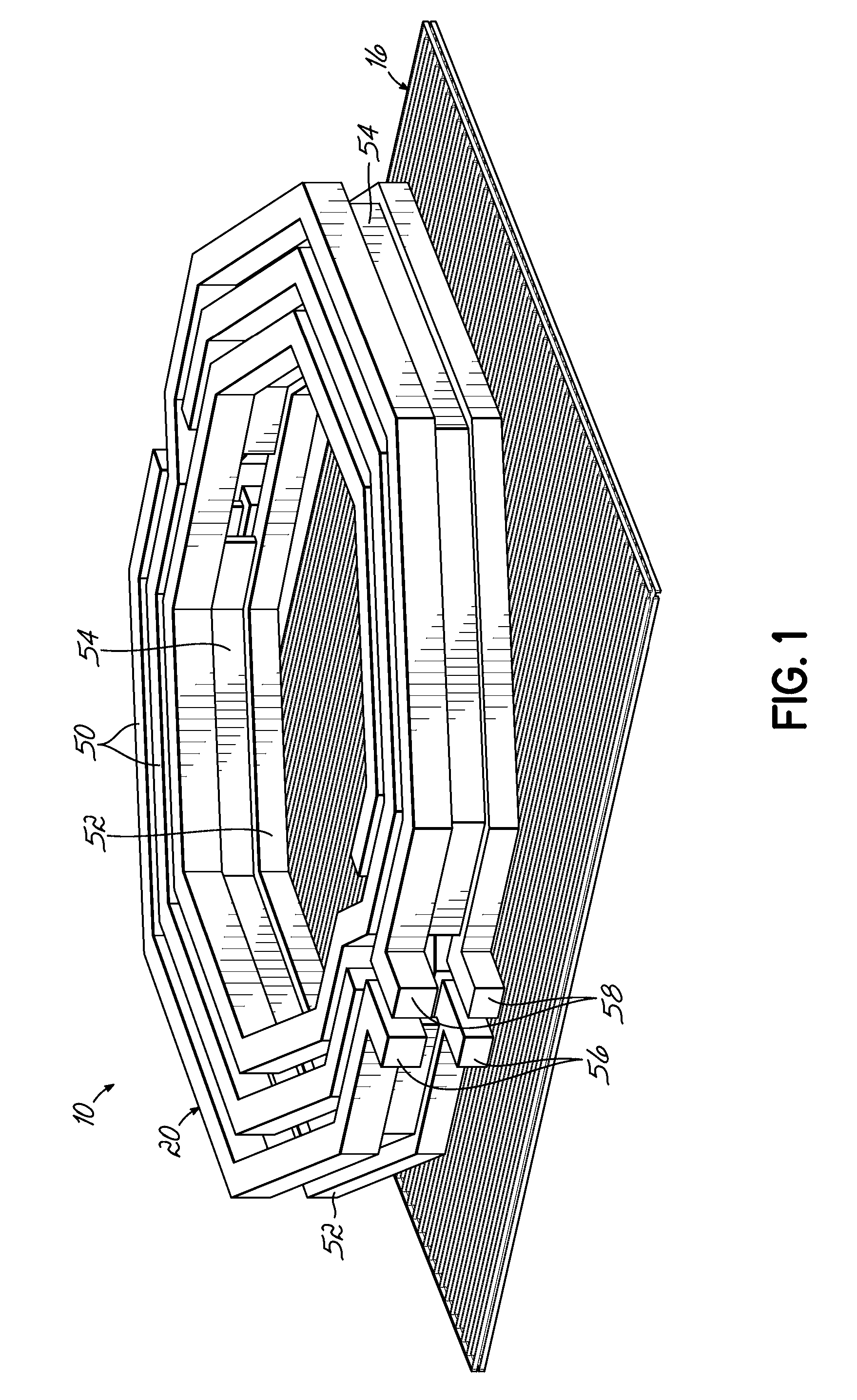
[0022]With reference to FIGS. 1, 2, 2A, 2B and in accordance with an embodiment of the invention, a back-end-of-line (BEOL) wiring structure, generally indicated by reference numeral 10, includes a dielectric layer 12 of a metallization level (Mx), a dielectric layer 14 of a metallization level (Mx−1) underlying the metallization level (Mx), an on-chip capacitor 16 embedded in the dielectric layers 12, 14, a dielectric layer 18 of an upper metallization level (Mx+1) overlying the metallization level (Mx), a dielectric layer 19 of an upper metallization level (Mx+2) overlying the metallization level (Mx−a), and an on-chip inductor 20 embedded in the dielectric layers 18, 19. Additional metallization levels (not shown) may exist below the metallization level (Mx−1), between metallization level (Mx) and metallization levels (Mx+1, Mx+2), and / or above the upper metallization levels (Mx+1, Mx+2). Conductive features in the different metallization levels of the BEOL wiring structure, such...
PUM
 Abstract
Description
Claims
Application Information