Method for page- and block based scrambling in non-volatile memory

a non-volatile memory and page-based scrambling technology, applied in the field of memory devices, can solve the problems of raising the threshold voltage of a storage element, errors can be caused during read operations, etc., and achieve the effect of significantly reducing the probability of errors and pattern length

Active Publication Date: 2009-12-31
SANDISK TECH LLC
View PDF12 Cites 174 Cited by
  • Summary
  • Abstract
  • Description
  • Claims
  • Application Information

AI Technical Summary

Benefits of technology

[0156]The computation is as follows. Once a specific cell is identified at state ‘E’ (in this case) then its four neighboring cells (in the BL, for example) have to have the same states, so we multiply by (¼)4. Further, the cell can appear in any of the five locations in the pattern so we multiply by ‘5’. Both cells at the edge of the pattern, i.e., before the pattern starts and after the pattern ends, and cannot hold state ‘E’; otherwise, the pattern length would be longer. Therefore they may have any of the other three states. The probability for that is (1¼)2]. Speci

Problems solved by technology

However, errors can be caused during read operations due to factors such as electromagnetic coupling between storage elements which is a function of the storage elements' respective data states.
S

Method used


Image

  • Method for page- and block based scrambling in non-volatile memory
  • Method for page- and block based scrambling in non-volatile memory
  • Method for page- and block based scrambling in non-volatile memory

Examples


Embodiment Construction

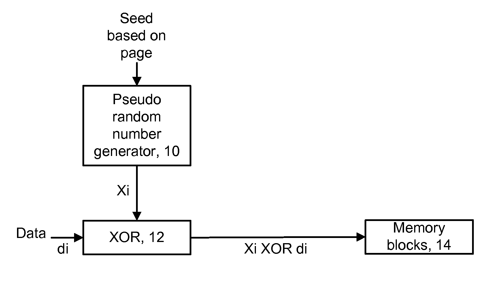
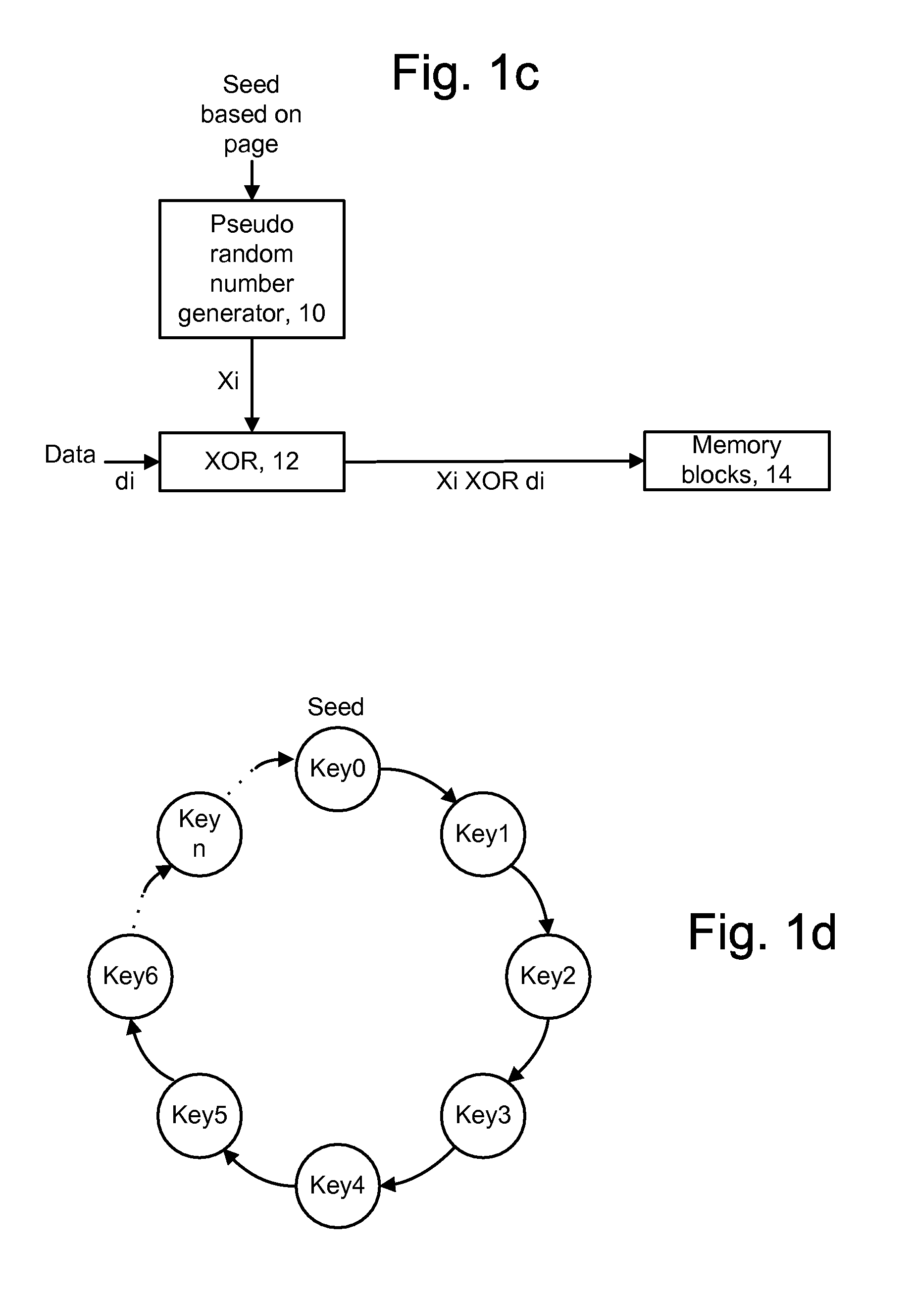
[0057]The present invention provides a method and system for programming and reading data with reduced errors in a memory device.

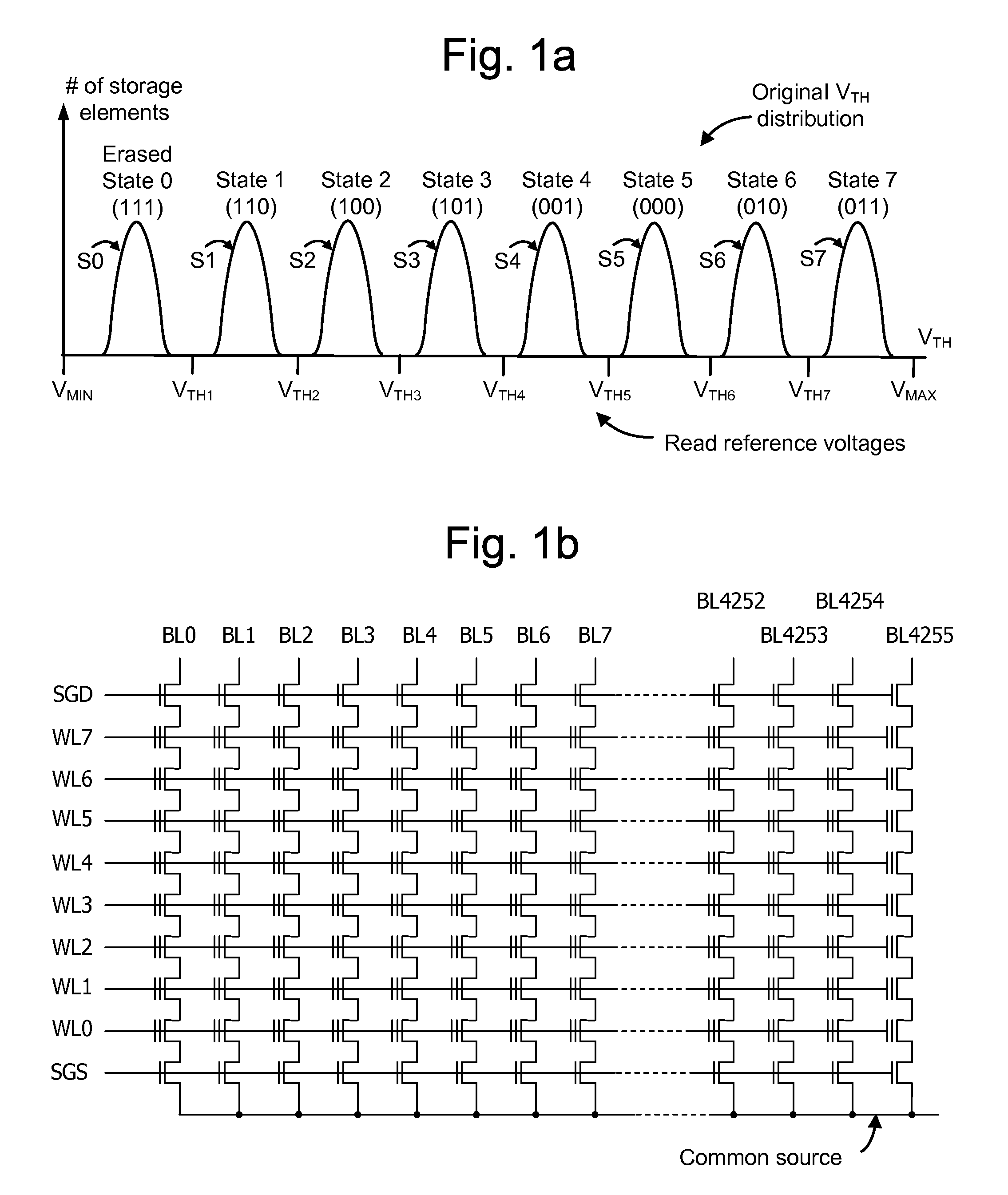
[0058]FIG. 1a depicts a threshold voltage distribution of a set of storage elements, a corresponding assignment to data states, and associated read reference voltages. The figure depicts an original or baseline threshold voltage (VTH) distribution which exists after a set of storage elements is programmed.

[0059]For historical reasons, writing data to a flash cell is called “programming” the flash cell. The terms “writing” and “programming” are used interchangeably herein. This is done by applying voltage pulses to the cell, to inject electrons from the cell's silicon substrate through the cell's oxide layer into the cell's floating gate, until the threshold voltage of the cell is high enough within the voltage window to represent the desired bit pattern. The threshold voltage of a flash cell is in a range, called the “voltage window,” as shown in FIG. 1a, ...


PUM


Abstract

A method and system for programming and reading data with reduced read errors in a memory device. In one approach, date to be written to the memory device is scrambled using a first pseudo random number which is generated based on a page of the memory device to which the data is to be written, to provide first scrambled data, which is scrambled using a second pseudo random number which is generated based on a block of the memory device to which the data is to be written. This avoids bit line-to-bit line and block-to-block redundancies which can result in read errors. The data may also be scrambled using a third pseudo random number that depends on a section within a page. Scrambling may also be based on one or more previous pages which were written.

Description

CROSS-REFERENCE TO RELATED APPLICATIONS[0001]This application claims the benefit of U.S. provisional patent application No. 61 / 076,791, filed Jun. 30, 2008, (docket no.: SAND-01358US0), incorporated herein by reference.BACKGROUND OF THE INVENTION[0002]1. Field of the Invention[0003]The present invention relates to a memory device.[0004]2. Description of the Related Art[0005]Semiconductor memory has become increasingly popular for use in various electronic devices. For example, non-volatile semiconductor memory is used in cellular telephones, digital cameras, personal digital assistants, mobile computing devices, non-mobile computing devices and other devices. Electrically Erasable Programmable Read Only Memory (EEPROM) and flash memory are among the most popular non-volatile semiconductor memories. During a programming or write operation, a series of program voltages is applied to a set of storage elements such as on a word line to raise the threshold voltages of the storage element...

Claims


Application Information

Patent Timeline
IPC IPC(8): H04L9/28H04L9/06
CPCG11C7/1006G11C11/5628G11C16/3427G11C16/3418G11C16/10
Inventor SHARON, ERANALROD, IDAN
Owner SANDISK TECH LLC
Why Eureka
Try Eureka