Waveguide photodetector device and manufacturing method thereof

a photodetector device and waveguide technology, applied in the field of optoelectronic devices, can solve the problems of increased interconnection delay, increased interconnection delay, electromagnetic interference (emi) and power consumption, and difficulty in integrating the photodetector device into the later stages of the integrated circuit fabrication process

Active Publication Date: 2009-12-31
INTEL CORP
View PDF65 Cites 68 Cited by
  • Summary
  • Abstract
  • Description
  • Claims
  • Application Information

AI Technical Summary

Problems solved by technology

However, the smaller dimensions of metal interconnect lead to undesirable effects such as increased interconnect delays, electromagnetic interference (EMI) and power consumption.
Furthermore, the photodetector device is made from part of a SOI substrate, which makes it difficult to integrate the photodetector device into later stages of an integrated circuit fabrication process.

Method used


Image

  • Waveguide photodetector device and manufacturing method thereof
  • Waveguide photodetector device and manufacturing method thereof
  • Waveguide photodetector device and manufacturing method thereof

Examples


Embodiment Construction

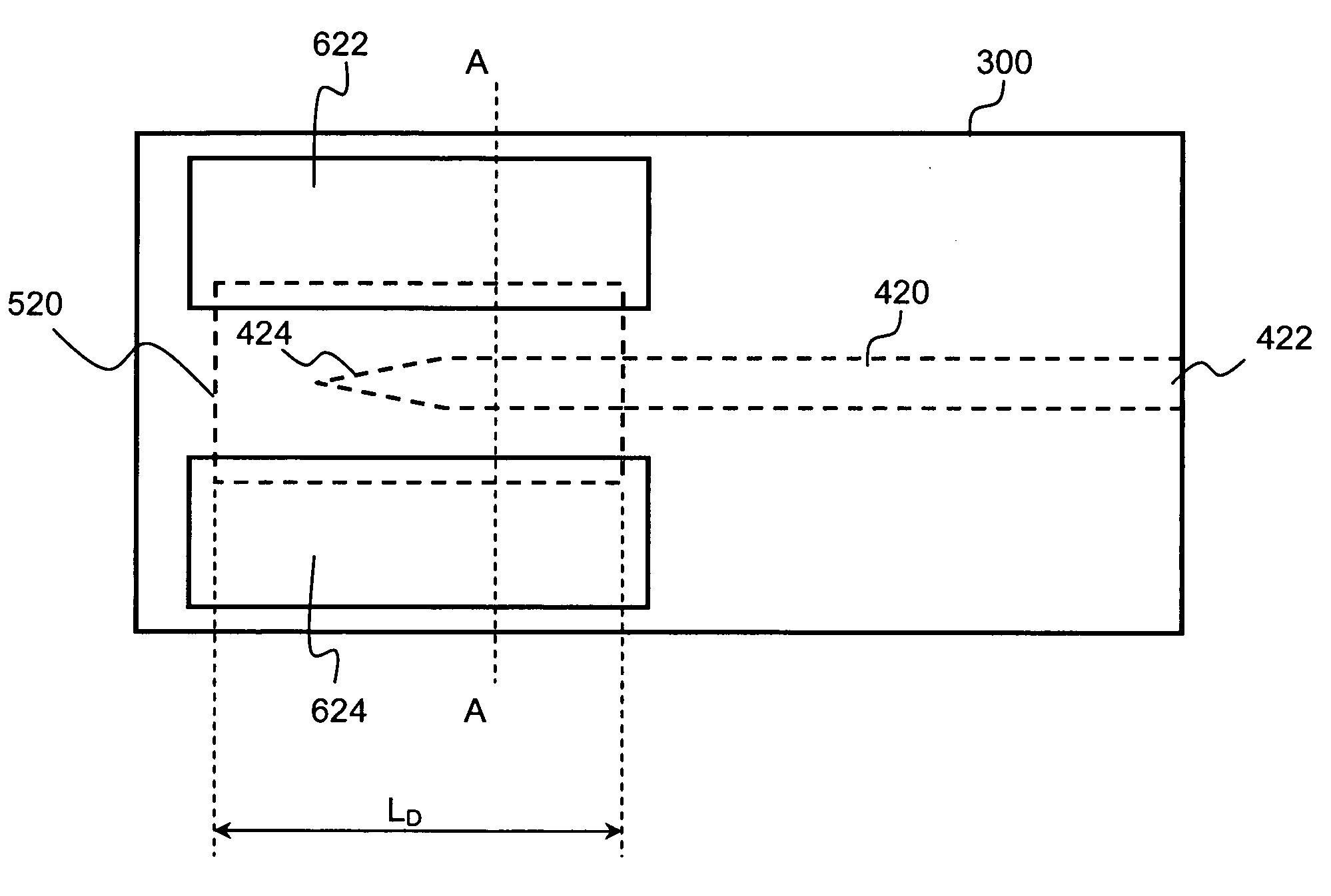
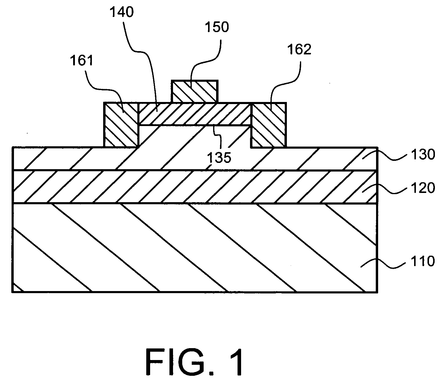
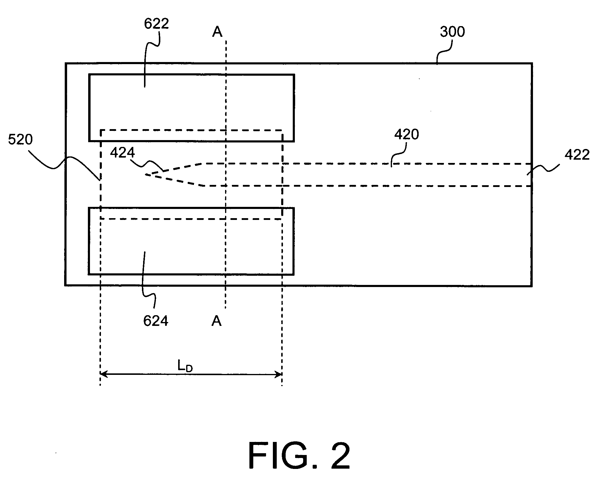
[0018]A waveguide-based photodetector device and its method of fabrication are described. In the following description, numerous specific details are set forth in order to provide a thorough understanding of the present invention. In other instances, well known semiconductor processing techniques and features have not been described in particular detail in order not to unnecessarily obscure the present invention.

[0019]Embodiments of the present invention describe a waveguide-based photodetector device and its methods of fabrication. In an embodiment of the present invention, the waveguide photodetector device comprises a substrate having a cladding structure formed thereon. A waveguide element for receiving optical signals is disposed within the cladding structure. The top surface and the portions of sidewalls of the waveguide element is encapsulated by a photodetector element that detects the optical signal received by the waveguide element and generates an electrical signal based ...


PUM


Abstract

Embodiments of the present invention describe a waveguide-based photodetector device and its methods of fabrication. The waveguide photodetector device comprises a substrate having a cladding structure formed thereon. A waveguide element for receiving optical signals is disposed within the cladding structure. A portion of the waveguide element is encapsulated by a photodetector element that detects the optical signal received by the waveguide element and generates an electrical signal based on the optical signal. Encapsulating the waveguide element in the photodetector element improves coupling efficiency and enables a waveguide photodetector device with higher speeds and higher responsivity.

Description

BACKGROUND OF THE INVENTION[0001]1. Field of the Invention[0002]The present invention relates to the field of optoelectronic devices and more particularly to a waveguide-based photodetector device and manufacturing method thereof.[0003]2. Discussion of Related Art[0004]Over recent years, the increasing computing power of integrated circuits, such as a microprocessor, has been enabled by downscaling the size of basic devices such as transistors and metal interconnects. However, the smaller dimensions of metal interconnect lead to undesirable effects such as increased interconnect delays, electromagnetic interference (EMI) and power consumption. In that regard, optical interconnects have been proposed as an alternative to metal interconnects. Optical interconnects have the advantages of being resistant to EMI and decrease interconnect delays and power consumption. Furthermore, the optical interconnect serves as a better alternative in keeping pace with increasing transistor speed as i...

Claims


Application Information

Patent Timeline
Patent Type & Authority Applications(United States)
IPC IPC(8): G02B6/12H01L21/00H01L31/00
CPCG02B6/1228G02B6/42H01L31/1085H01L31/105G02B6/4202
Inventor RESHOTKO, MIRIAM R.BLOCK, BRUCE A.
Owner INTEL CORP
Why Eureka
Try Eureka