Transparent conductive layer and method of manufacturing the same

a technology of transparent conductive layer and manufacturing method, which is applied in the direction of solid-state devices, basic electric elements, and negative resistance devices, can solve the problem of low light generation efficiency of electron-hole pairs, and achieve the effect of enhancing light efficiency and increasing light scattering

Inactive Publication Date: 2010-01-07
SAMSUNG DISPLAY CO LTD +1
View PDF0 Cites 14 Cited by
  • Summary
  • Abstract
  • Description
  • Claims
  • Application Information

AI Technical Summary

Benefits of technology

[0012]The disclosed transparent conductive layer, and method of manufacturing the same, increases light scattering in a long wavelength region, enhances a light efficiency, and includes a first conductive layer and a second conductive layer, which can be sequentially disposed on a substrate, wherein the second conductive layer includes an opening, which exposes the first conductive layer, and a top surface of the second conductive layer is a textured surface.
[0029]In an exemplary embodiment, etching of an In2O3-based first conductive layer can be substantially reduced or prevented, a selected sheet resistance provided, and a ZnO-based second conductive layer can include a dual texture structure to thereby increase light scattering in a long wavelength region. Consequently, the light efficiency of a photoelectric device can be improved.

Problems solved by technology

Also, if the thin film solar cell is fabricated only with a PN junction structure, the collection efficiency of light generated electron-hole pairs is low.

Method used


Image

  • Transparent conductive layer and method of manufacturing the same
  • Transparent conductive layer and method of manufacturing the same
  • Transparent conductive layer and method of manufacturing the same

Examples


Embodiment Construction

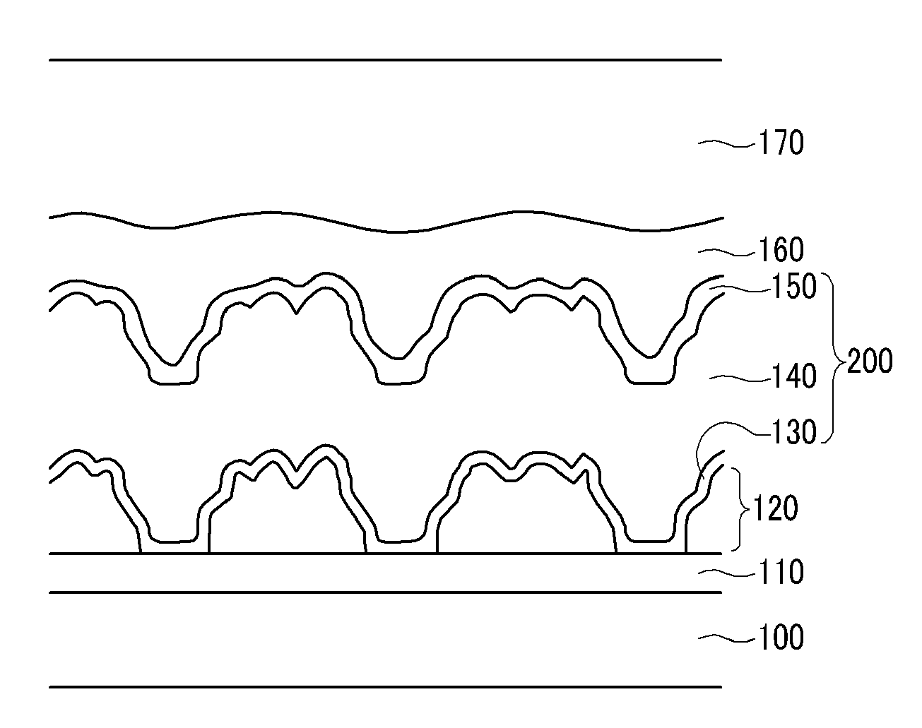
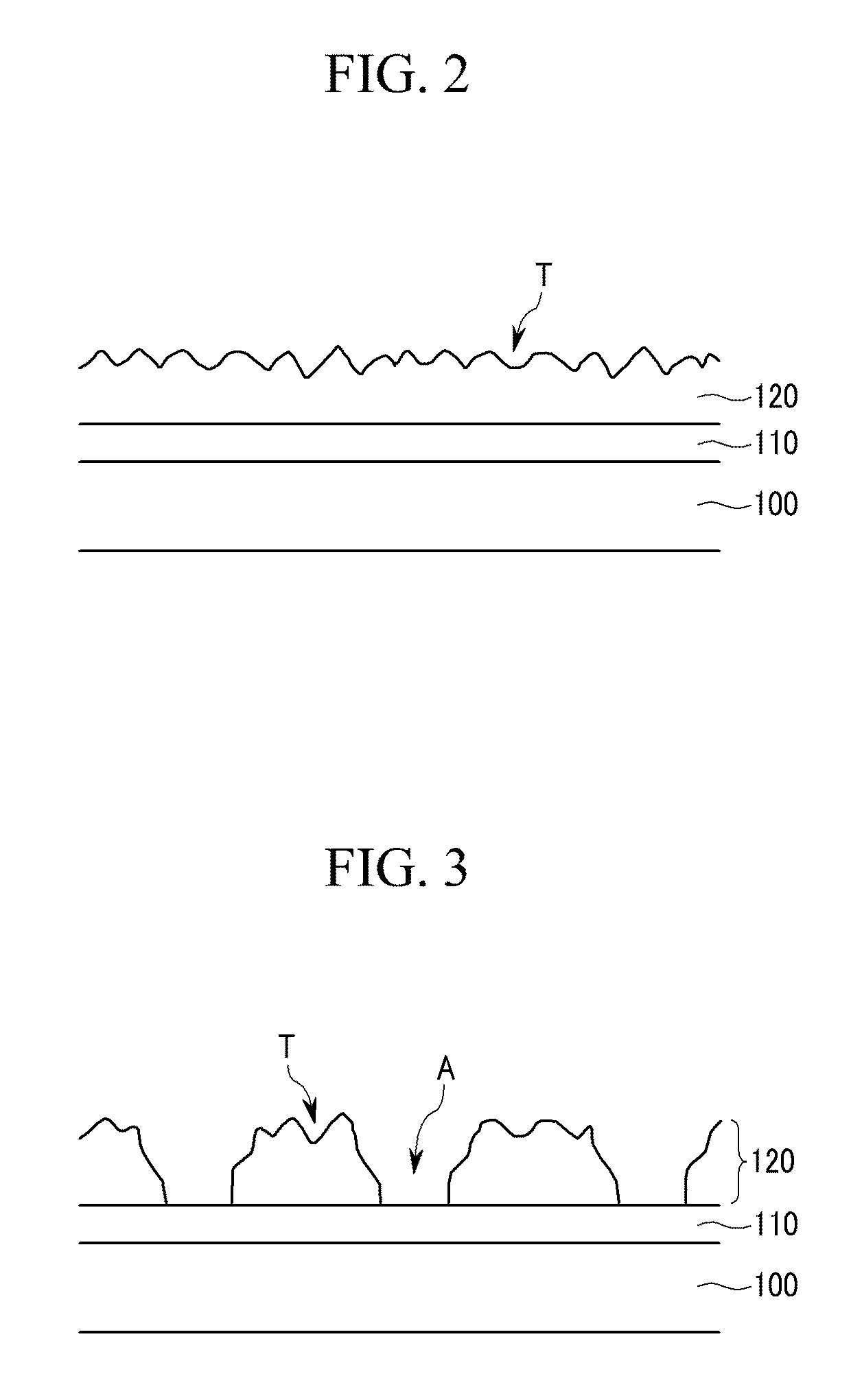
[0039]The exemplary embodiments are described more fully hereinafter with reference to the accompanying drawings, in which exemplary embodiments are shown. As those skilled in the art would realize, the described embodiments may be modified in various ways, all without departing from the spirit or scope of the invention.

[0040]In the drawings, the thickness of layers, films, panels, regions, etc., are exaggerated for clarity. It will be understood that when an element such as a layer, film, region, or substrate is referred to as being “on” another element, it can be directly on the other element or intervening elements may also be present. Like reference numerals designate like elements throughout the specification.

[0041]The terms “the”, “a” and “an” do not denote a limitation of quantity, but rather denote the presence of at least one of the referenced item.

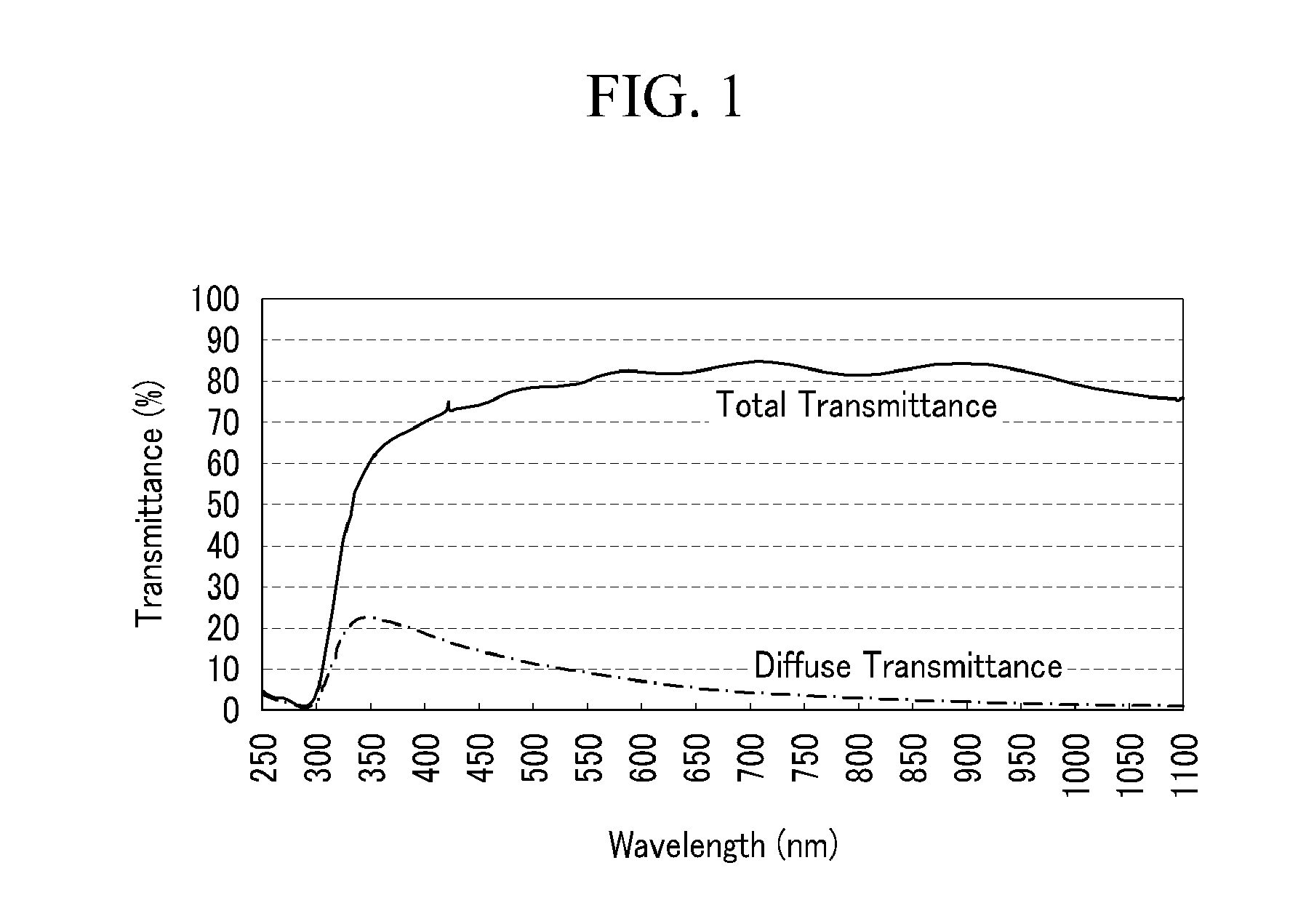
[0042]A diffuse transmittance can be defined as the degree by which a direction of light progression is varied when light passe...


PUM

PropertyMeasurementUnit
diameteraaaaaaaaaa
thicknessaaaaaaaaaa
thicknessaaaaaaaaaa

Abstract

A transparent conductive layer includes a substrate, a first conductive layer disposed on the substrate, and a second conductive layer disposed on the first conductive layer, wherein the second conductive layer comprises a textured surface and an opening which exposes the first conductive layer, wherein the opening comprises a diameter of about 1 micrometer to about 3 micrometers. Also disclosed is a method of manufacturing the transparent conductive layer and a photoelectric device.

Description

[0001]This application claims priority to Korean Patent Application No. 10-2008-0065078, filed on Jul. 4, 2008, and all the benefits accruing therefrom under 35 U.S.C. §119, the contents of which in its entirety are herein incorporated by reference.BACKGROUND OF THE INVENTION[0002](a) Field of the Invention[0003]This disclosure relates to a transparent conductive layer and a method of manufacturing the same.[0004](b) Description of the Related Art[0005]A photoelectric device, such as a solar cell, converts light energy into electric energy. Types of photoelectric devices can be differentiated by the metals used therein for the active layers. Thus a solar cell converts solar energy into electric energy, and generates electricity using at least two kinds of semiconductors, a P-type semiconductor, and an N-type semiconductor.[0006]Classes of solar cells include crystalline silicon solar cells, which are commercially available, thin film solar cells, which are based on low cost substrat...

Claims


Application Information

Patent Timeline
Patent Type & Authority Applications(United States)
IPC IPC(8): H01L31/0224H01L23/532H01L21/28
CPCH01L31/022466Y02E10/50H01L31/1884H01L31/0236H01L31/022483H01L31/02366Y02E10/548H01L31/0224H01L31/04H01L31/18
Inventor JUNG, SEUNG-JAENAM, YUK-HYUNLEE, CZANG-HOSHIN, MYUNG-HUNOH, MIN-SEOKLEE, BYOUNG-KYULIM, MI-HWASEO, JOON-YOUNG
Owner SAMSUNG DISPLAY CO LTD
Why Eureka
Try Eureka