Magnetic tunnel junction device, memory cell having the same, and method for fabricating the same

a tunnel junction device and memory cell technology, applied in the direction of magnetic-field-controlled resistors, semiconductor devices, electrical devices, etc., can solve the problems of deterioration of mtj devices, and inability of mtj devices to operate normally

Inactive Publication Date: 2010-01-07
SK HYNIX INC
View PDF12 Cites 53 Cited by
  • Summary
  • Abstract
  • Description
  • Claims
  • Application Information

AI Technical Summary

Benefits of technology

[0008]Embodiments of the present invention are directed to provide a magnetic tunnel junction device capable of preventing interference phenomenon and electrical short between adjacent MTJ devices and a method for fabricating the same.
[0009]Embodiments of the present invention are also directed to provide an MTJ device capable of preventing characteristic deterioration of the MTJ device, which may be caused by a conductive etch byproduct occurring during an etch process for forming the MTJ device.

Problems solved by technology

As the interval between adjacent MTJ devices is decreased, interference phenomenon therebetween may occur, where characteristics of the MTJ device are deteriorated.
Additionally, when the interval S2 between adjacent MTJ devices is decreased even more, electrical short therebetween may occur, where characteristics of the MTJ device are deteriorated or the MTJ device cannot operate normally.
These conditions worsen as dimensions of a semiconductor device are reduced based on design needs.
Moreover, as shown in ‘X’ of FIG. 1, an etch byproduct 109 occurring during an etch process for forming the MTJ device may be re-deposited on the sidewall of the MTJ device, such that characteristics of the MTJ device are deteriorated.
Especially, when the conductive etch byproduct is re-deposited on the sidewall of the free layer 106 and the pinned layer 104, electrical short occurs therebetween such that characteristics of the MTJ device are deteriorated or the MTJ device cannot operate normally in severe conditions.

Method used


Image

  • Magnetic tunnel junction device, memory cell having the same, and method for fabricating the same
  • Magnetic tunnel junction device, memory cell having the same, and method for fabricating the same
  • Magnetic tunnel junction device, memory cell having the same, and method for fabricating the same

Examples


first embodiment

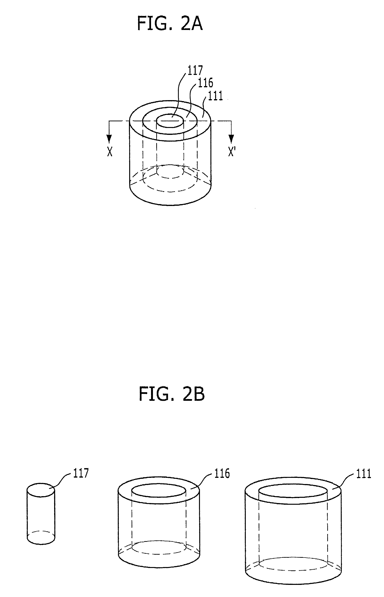
[0032]FIGS. 2A to 2D illustrate an MTJ device in accordance with the present invention. FIG. 2A is a perspective view of a unit of the MTJ device. FIG. 2B is a perspective view illustrating each separated component of an MTJ device. FIG. 2C is a cross-sectional view taken along a line X-X′. FIG. 2D is a cross-sectional view illustrating an MTJ device having a concave structure. Referring to FIGS. 2A to 2D, the MTJ device of the present invention has a pillar-type concave structure. Specifically, the MTJ device includes a pillar-type second electrode 117, an MTJ layer 116 surrounding the side and the bottom of the second electrode 117, and a first electrode 111 surrounding the side and the bottom of the second MTJ layer 116. Herein, the second electrode 117 may have a circular cylinder shape, a tri-cylinder shape, or a polygonal cylinder shape. Additionally, the first electrode 111 and the MTJ layer 116 may have a cylindrical shape.

[0033]Additionally, the MTJ device of the present in...

second embodiment

[0058]Hereafter, a memory cell including the pillar-type MTJ device of the present invention will be described with reference to the accompanying drawings. In general, an MR ratio of the MTJ device is determined by a magnetization direction of a free layer. Accordingly, based on a driving principle (for example, a magnetic field or STT) that changes a magnetization direction of the free layer, a structure of a memory cell including the MTJ device may be different. In the present invention that will be mentioned later, a memory cell using STT as a driving principle for changing a magnetization direction of a free layer is exemplified. In this disclosure, the STT can be described with reaction of giant magnetoresistive (GMR). According to Newton's third law (that is, a law of action and reaction), action is inevitably followed by corresponding reaction having the same magnitude and a reverse direction to the action. Herein, the GMR is a phenomenon that occurs because a current amount ...

third embodiment

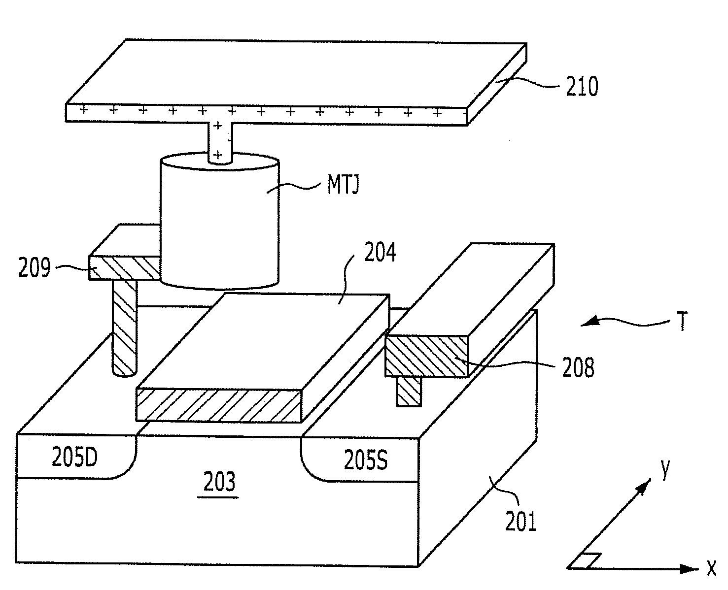
[0075]FIG. 6A is a cross-sectional view illustrating a memory cell with an MTJ device in accordance with the present invention. FIG. 6B is a perspective view illustrating a unit cell of the memory cell of FIG. 6A. Referring to FIGS. 6A and 6B, a device isolation layer 202 is disposed on a predetermined region of a substrate 201 to define an active region 203. A plurality of gate electrodes 204 (that is, a word line) crossing over the active region 203 and the device isolation layer 202 at the same time are disposed on the substrate 201 including the device isolation layer 202. Herein, when a direction of the active region 203 is designated as a row direction which is the x-axis direction, a gate electrode 204 is disposed in a column direction which is the y-axis direction. A common source region 205S is disposed in the substrate 201 of the active region 203 between the gate electrodes 204, and a drain region 205D is disposed in the substrate 201 of the active region 203 at both side...


PUM


Abstract

A method for fabricating a magnetic tunnel junction device includes forming an insulation layer having a plurality of openings, forming a first electrode over the bottom and the sidewall of an opening of the plurality of openings, forming a magnetic tunnel junction layer over the first electrode, and forming a second electrode over the magnetic tunnel junction layer to fill the remaining openings.

Description

CROSS-REFERENCE TO RELATED APPLICATIONS[0001]The present invention claims priority of Korean patent application number 10-2008-0064396, filed on Jul. 3, 2008, the disclosure of which is incorporated herein by reference in its entirety.BACKGROUND OF THE INVENTION[0002]The present invention relates to a semiconductor device fabricating method, and more particularly, to a magnetic tunnel junction (MTJ) device capable of preventing interference phenomenon between adjacent MTJ devices, a memory cell having the same, and a method for fabricating the same.[0003]As a semiconductor device is becoming highly integrated, a magnetic random access memory (MRAM) is considered as the next generation semiconductor memory device having advantages such as simple cell region reduction, a high speed operation, and non-volatility. The MRAM includes a transistor for performing a switching operation and an MTJ device for storing information. In relation to the MTJ device, a magnetoresistance (MR) ratio is...

Claims


Application Information

Patent Timeline
Patent Type & Authority Applications(United States)
IPC IPC(8): H01L21/00
CPCH01L27/226H01L43/12H01L43/08H10B61/22H10N50/01H10N50/10H01L27/105
Inventor CHO, SANG-HOON
Owner SK HYNIX INC
Why Eureka
Try Eureka