Thin film transistor, method of manufacturing the same and flat panel display device having the same

a technology of thin film transistors and flat panels, applied in non-linear optics, instruments, optics, etc., can solve the problems of difficult application of methods to larger substrates, difficult to implement high-speed driving circuits, and expensive processes, and achieve the effect of improving damage resistan

Active Publication Date: 2010-01-14
SAMSUNG DISPLAY CO LTD
View PDF35 Cites 148 Cited by
  • Summary
  • Abstract
  • Description
  • Claims
  • Application Information

AI Technical Summary

Benefits of technology

[0011]Aspects of the present invention provide a thin film transistor having improved damage resistance, during the formation

Problems solved by technology

However, if an activation layer is formed of amorphous silicon, it is difficult to implement a high speed driving circuit, due to it having low electron mobility.
A conventional method of manufacturing a thin film transistor, using a low temperature poly-silicon (LTPS), involves an expensive process such as a laser anneal

Method used


Image

  • Thin film transistor, method of manufacturing the same and flat panel display device having the same
  • Thin film transistor, method of manufacturing the same and flat panel display device having the same
  • Thin film transistor, method of manufacturing the same and flat panel display device having the same

Examples


Embodiment Construction

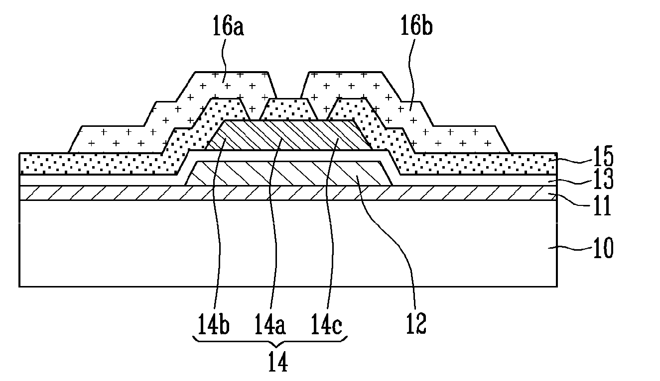
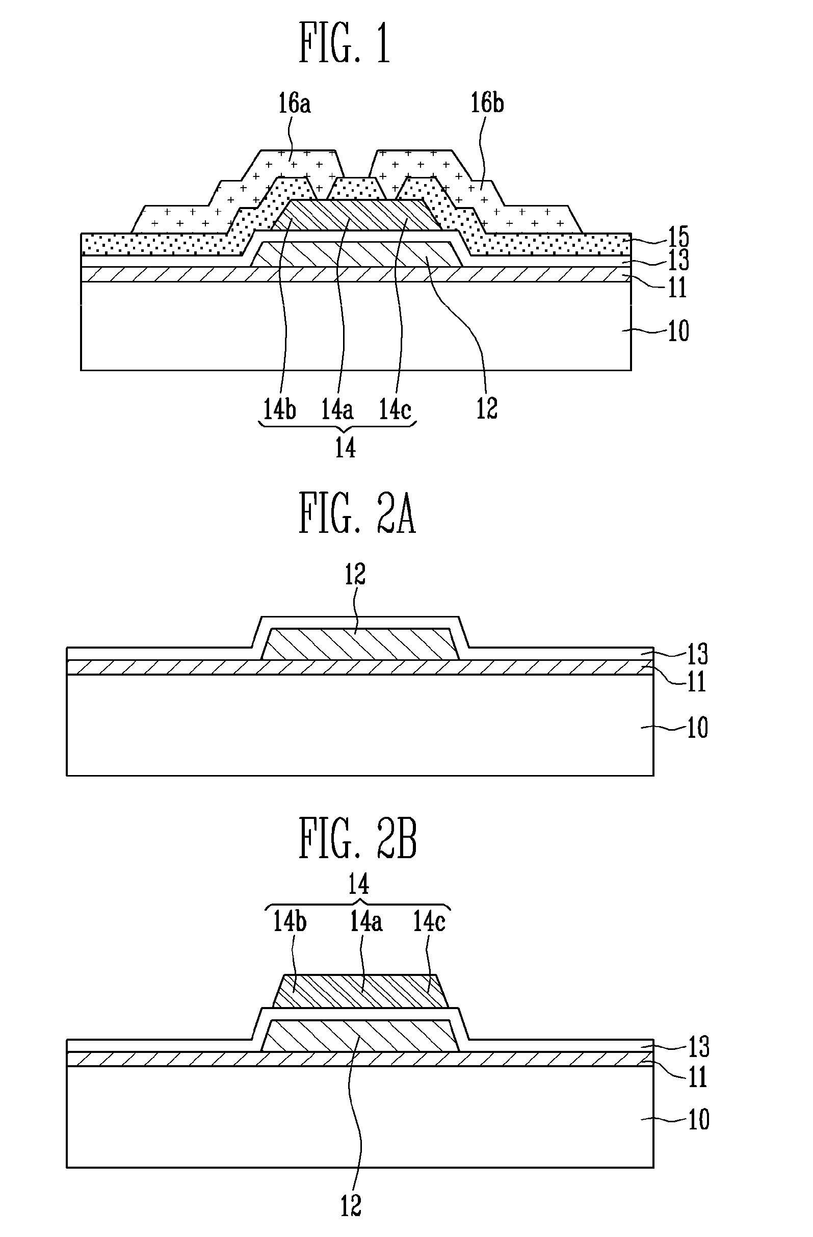
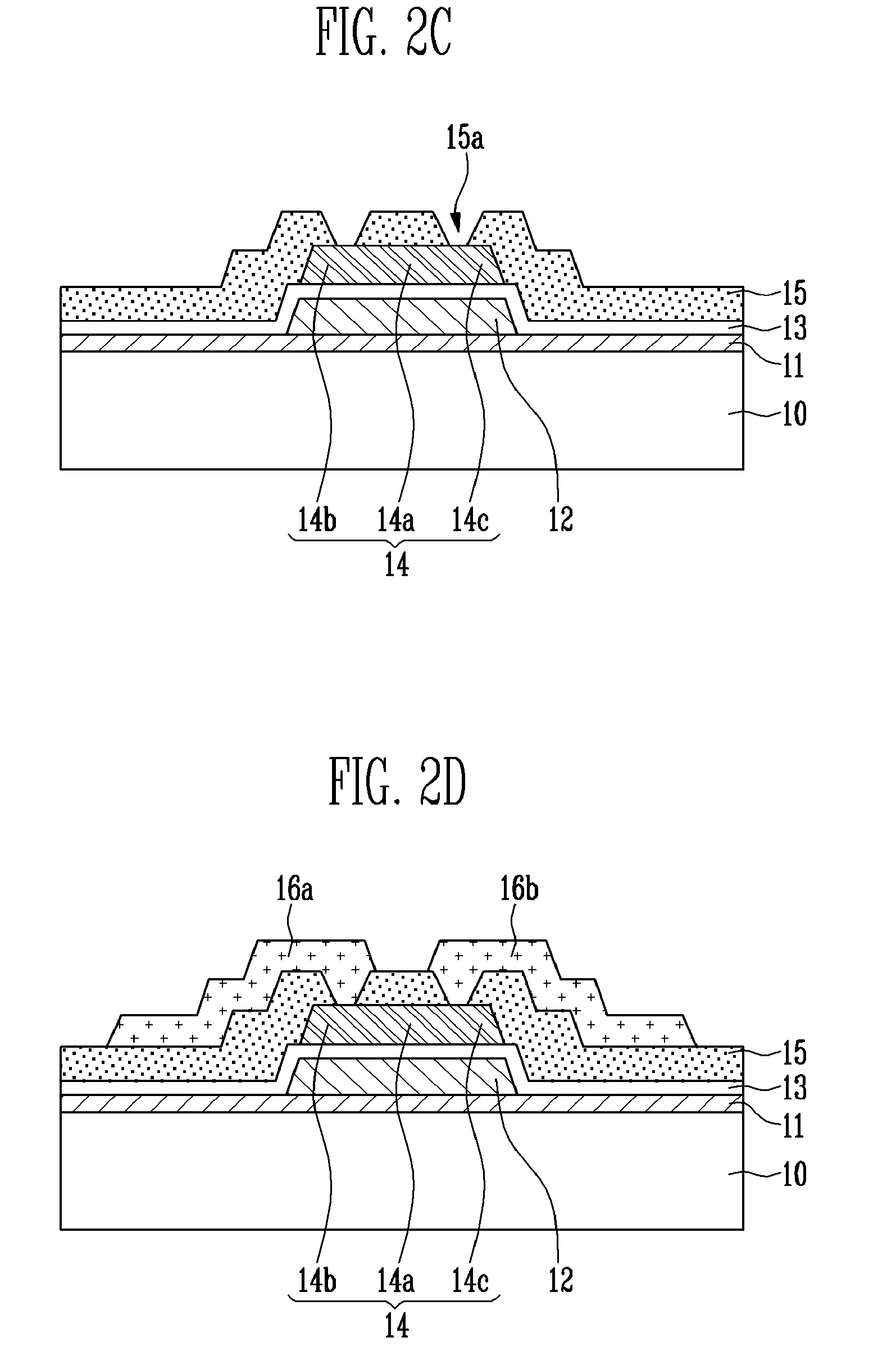
[0033]Reference will now be made in detail to the exemplary embodiments of the present invention, examples of which are illustrated in the accompanying drawings, wherein like reference numerals refer to the like elements throughout. The exemplary embodiments are described below, in order to explain the aspects of the present invention, by referring to the figures. The described exemplary embodiments may be modified in various different ways, without departing from the spirit or scope of the present invention. Accordingly, the drawings and description are to be regarded as illustrative in nature and not restrictive. In addition, when an element is referred to as being “on” another element, it can be directly on another element or can be indirectly on the element with one, or one or more intervening elements can be interposed therebetween. Also, when an element is referred to as being “connected to” another element, it can be directly connected to the element, or can be indirectly con...


PUM


Abstract

A thin film transistor, a method of manufacturing the thin film transistor, and a flat panel display device including the thin film transistor. The thin film transistor includes: a gate electrode formed on a substrate; a gate insulating film formed on the gate electrode; an activation layer formed on the gate insulating film; a passivation layer including a compound semiconductor oxide, formed on the activation layer; and source and drain electrodes that contact the activation layer.

Description

CROSS-REFERENCE TO RELATED APPLICATION[0001]This application claims the benefit of Korean Patent Application No. 2008-66002, filed on Jul. 8, 2008, in the Korean Intellectual Property Office, the disclosure of which is incorporated herein, by reference.BACKGROUND OF THE INVENTION[0002]1. Field of the Invention[0003]Aspects of the present invention relate to a thin film transistor, a method of manufacturing the same, and a flat panel display device including the same.[0004]2. Description of the Related Art[0005]A thin film transistor generally includes: an activation layer including a channel region, a source region, and a drain region; and a gate electrode which is formed on the channel region. The gate electrode is electrically insulated from the activation layer, by a gate insulating film.[0006]An activation layer is generally formed of semiconductor material, such as amorphous silicon or poly-silicon. However, if an activation layer is formed of amorphous silicon, it is difficult...

Claims


Application Information

Patent Timeline
IPC IPC(8): H01L29/12H01L21/04H05B44/00
CPCH01L29/7869G02F1/1368H01L29/78606H01L29/78696H10K59/1213
Inventor HA, JAE-HEUNGSONG, YOUNG-WOOLEE, JONG-HYUKJEONG, JONG-HANKIM, MIN-KYUMO, YEON-GONJEONG, JAE-KYEONGCHUNG, HYUN-JOONGKIM, KWANG-SUKYANG, HUI-WONCHOI, CHAUN-GI
Owner SAMSUNG DISPLAY CO LTD
Why Eureka
Try Eureka