Optical element and method for producing same

Inactive Publication Date: 2010-04-29
SEIKO EPSON CORP
View PDF0 Cites 23 Cited by
  • Summary
  • Abstract
  • Description
  • Claims
  • Application Information

AI Technical Summary

Benefits of technology

[0065]According to a second aspect, there is provided a method for producing an optical element. The method includes preparing a first optical component and a second optical component each having light transmission properties and being adapted to be bonded together via a bonding film to form an optical element and forming the bonding film on a surface of the first optical component by plasma polymerization, the bonding film including an Si skeleton having a random atomic structure including a siloxane (Si—O) bond and leaving groups binding to the Si skeleton; applying energy to the bonding film to eliminate the leaving groups from the Si sk

Problems solved by technology

However, in general, the refractive index of an adhesive tends to be uniquely determined in accordance with a composition of the adhesive, so that it is difficult of adjust the refractive index to an arbitrary value.
Usually, however, such an additive is added during production of the adhe

Method used


Image

  • Optical element and method for producing same
  • Optical element and method for producing same
  • Optical element and method for producing same

Examples


first embodiment

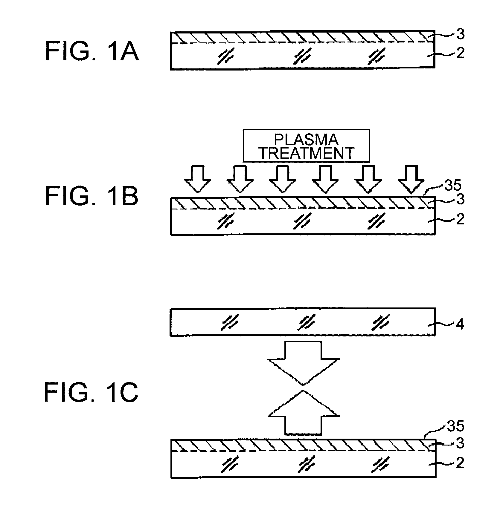
[0082]Next, a description will be given of a method for producing an optical element according to a first embodiment.

[0083]FIGS. 1A to 2E are longitudinal sectional views explaining the production method of the first embodiment. In the description below, upper and lower sides, respectively, in FIGS. 1A to 2E, will be referred to as “top” and “bottom”, respectively.

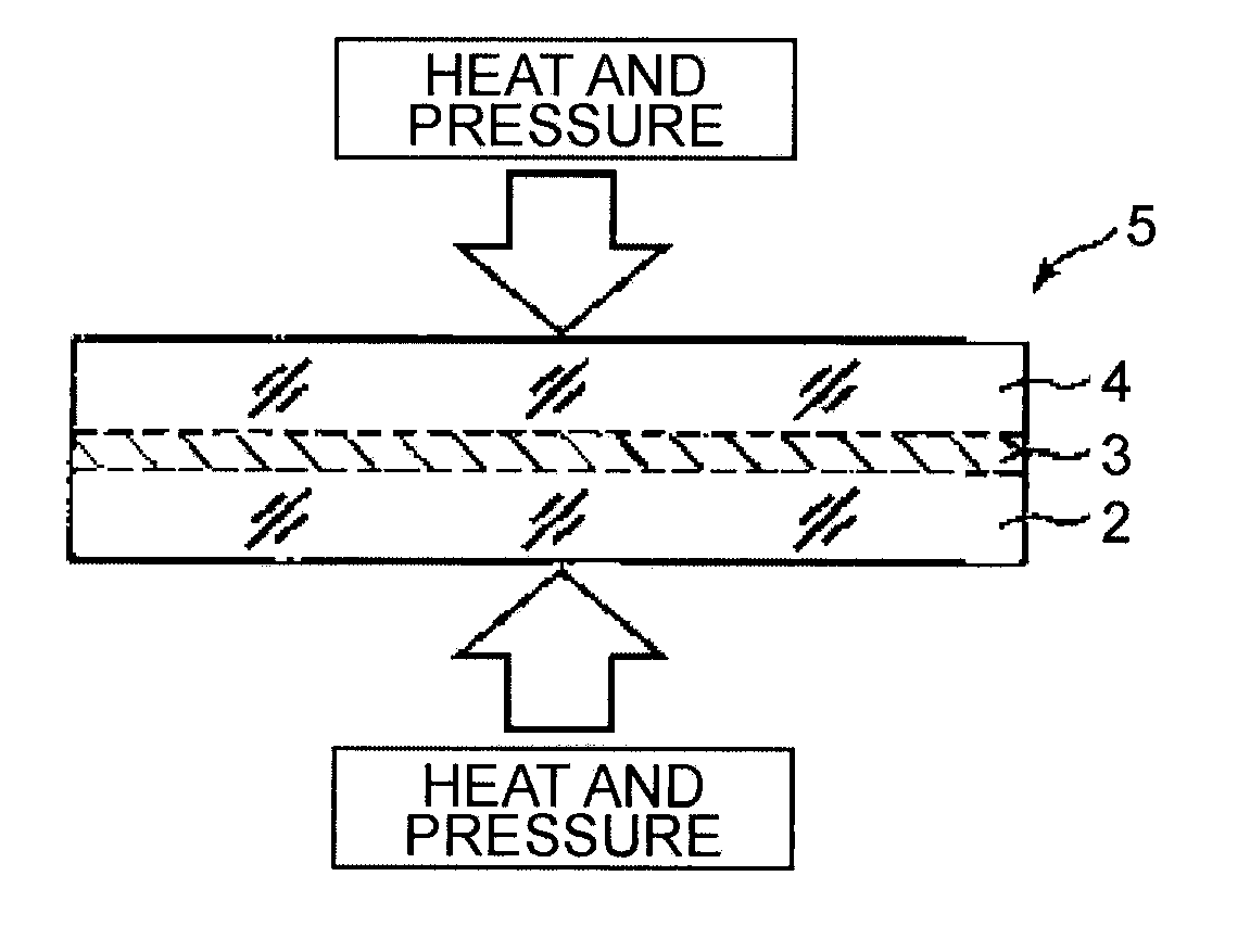
[0084]The method for producing an optical element of the first embodiment includes preparing the first and the second optical components 2 and 4 to form the bonding film 3 on a surface of the first optical component 2 by plasma polymerization (step 1); applying energy to the bonding film 3 (step 2); and bonding together the first and the second optical components 2 and 4 via the bonding film 3 to obtain a multi-layered optical element 5 (step 3). The steps will be sequentially described below.

[0085]1. First, the first and the second optical components 2 and 4 are prepared.

[0086]The optical components 2 and 4 are bonded tog...

second embodiment

[0246]Next, a description will be given of a method for producing an optical element according to a second embodiment.

[0247]FIGS. 7A to 7D are longitudinal sectional views explaining the method for producing an optical element according to the second embodiment. In the description below, upper and lower sides, respectively, in FIGS. 7A to 7D, will be referred to as “top” and “bottom”, respectively.

[0248]Hereinafter, the description of the method of the second embodiment will focus on points that are different from the first embodiment, whereas descriptions of the same points as in the first embodiment will be omitted.

[0249]The method of the second embodiment is the same as the method of the first embodiment except that a bonding film is formed on a surface of each of the optical components 2 and 4 to bond the components 2 and 4 together such that the bonding films are closely adhered to each other.

[0250]Specifically, the method for producing an optical element according to the secon...

example 1

[0285]First, each quartz crystal substrate was prepared for each of the first and the second optical components. The quartz crystal substrate for the first optical component had a length of 20 mm, a width of 20 mm, and a mean thickness of 2 mm, and the quartz crystal substrate for the second optical component 4 had a length of 20 mm, a width of 20 mm, and a mean thickness of 1 mm. The quartz crystal substrates were subjected to optical polishing. The quartz crystal substrates had a refractive index of 1.546 with respect to light having a wavelength of 546 nm.

[0286]Then, each of the substrates was placed in the chamber 101 of the plasma polymerization apparatus 100 shown in FIG. 5 to perform surface treatment using oxygen plasma.

[0287]Next, on a surface of each substrate subjected to the surface treatment was formed a plasma-polymerized film having a mean thickness of 150 nm. Conditions for formation of the film were as follows:

[0288]Conditions for Formation of Film

[0289]Composition ...


PUM

PropertyMeasurementUnit
Fractionaaaaaaaaaa
Thicknessaaaaaaaaaa
Wavelengthaaaaaaaaaa

Abstract

An optical element includes a first optical component and a second optical component each having light transmission properties; and a bonding film bonding together the first and the second optical components. The bonding film is formed by plasma polymerization and includes an Si skeleton having a random atomic structure including a siloxane (Si—O) bond and leaving groups binding to the Si skeleton. The first and the second optical components are bonded together by the bonding film having adhesive properties provided by applying energy to at least a part of the bonding film to eliminate the leaving groups from the Si skeleton at a surface of the bonding film. Additionally, the bonding film is formed so as to have approximately the same refractive index as that of at least one of the first and the second optical components by adjusting a film forming condition of the plasma polymerization.

Description

[0001]The entire disclosure of Japanese Patent Application No. 2008-277466, filed Oct. 28, 2008 is expressly incorporated by reference herein.BACKGROUND[0002]1. Technical Field[0003]The present invention relates to an optical element and a method for producing the optical element.[0004]2. Related Art[0005]Conventionally, two members (substrates) are bonded (adhesively bonded) together by an adhesive such as an epoxy, urethane, or silicone.[0006]The adhesives can exhibit adhesion properties regardless of the material of the members to be bonded together and thus can achieve bonding between various combinations of members made of different materials.[0007]For example, a wavelength plate is an optical element providing a phase difference to light transmitted therethrough. The wavelength plate is formed by combining two sheets of substrates made of birefringent crystal such as quartz crystal. The substrates are bonded together by an adhesive.[0008]When bonding together the substrates by...

Claims


Application Information

Patent Timeline
IPC IPC(8): B32B38/00
CPCC03C27/06C04B37/005C04B2235/483C04B2237/062G02B5/3083C04B2237/341C04B2237/345C04B2237/36G02B1/12C04B2237/34
Inventor OTSUKA, KENJIMATSUO, YASUHIDESAWAI, TAKENORI
Owner SEIKO EPSON CORP
Why Eureka
Try Eureka