Semiconductor device, method for manufacturing semiconductor device, method for manufacturing semiconductor package

Active Publication Date: 2010-01-14
TAIWAN SEMICON MFG CO LTD
View PDF12 Cites 39 Cited by
  • Summary
  • Abstract
  • Description
  • Claims
  • Application Information

AI Technical Summary

Benefits of technology

[0017]In accordance with the semiconductor device and the method for manufacturing a semiconductor device of the present invention, dishing of the STI region can be prevented by a dummy pattern formed in the non-active area. The Through Silicon VIA electrode formation area of the non-active area has a dummy pattern formed so that no area is generated wherein the outer edge of the Through Silicon VIA electrode intersects the dummy section. Therefore, etchin

Problems solved by technology

Difficulties arise in later steps because the flatness of the substrate is detracted when dishing occurs.
However, there is a problem in that notches (outwardly expanding depressions in the side wall of the Through Silicon VIA hole) are generated in the sidewall of the Through Silicon VIA holes when Through Silicon VIA holes are formed so as to pass through the non-active area in which the plurality of dummy actives are uniformly disposed.
However, Because Cu is a typical material that constitutes metal contamination in the silicon device and diffuses into the silicon substrate and the interlayer insulating film at lower temperat

Method used


Image

  • Semiconductor device, method for manufacturing semiconductor device, method for manufacturing semiconductor package
  • Semiconductor device, method for manufacturing semiconductor device, method for manufacturing semiconductor package
  • Semiconductor device, method for manufacturing semiconductor device, method for manufacturing semiconductor package

Examples


Embodiment Construction

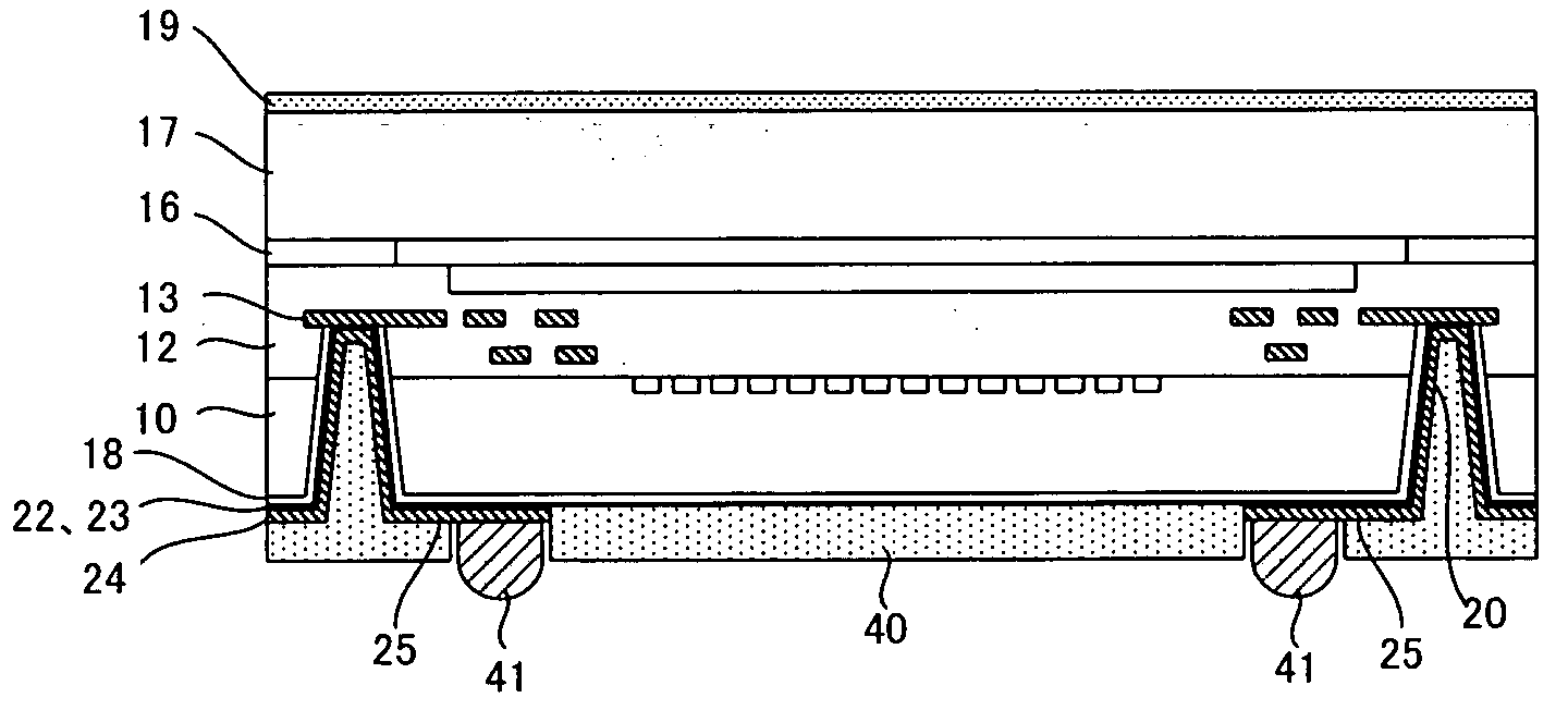
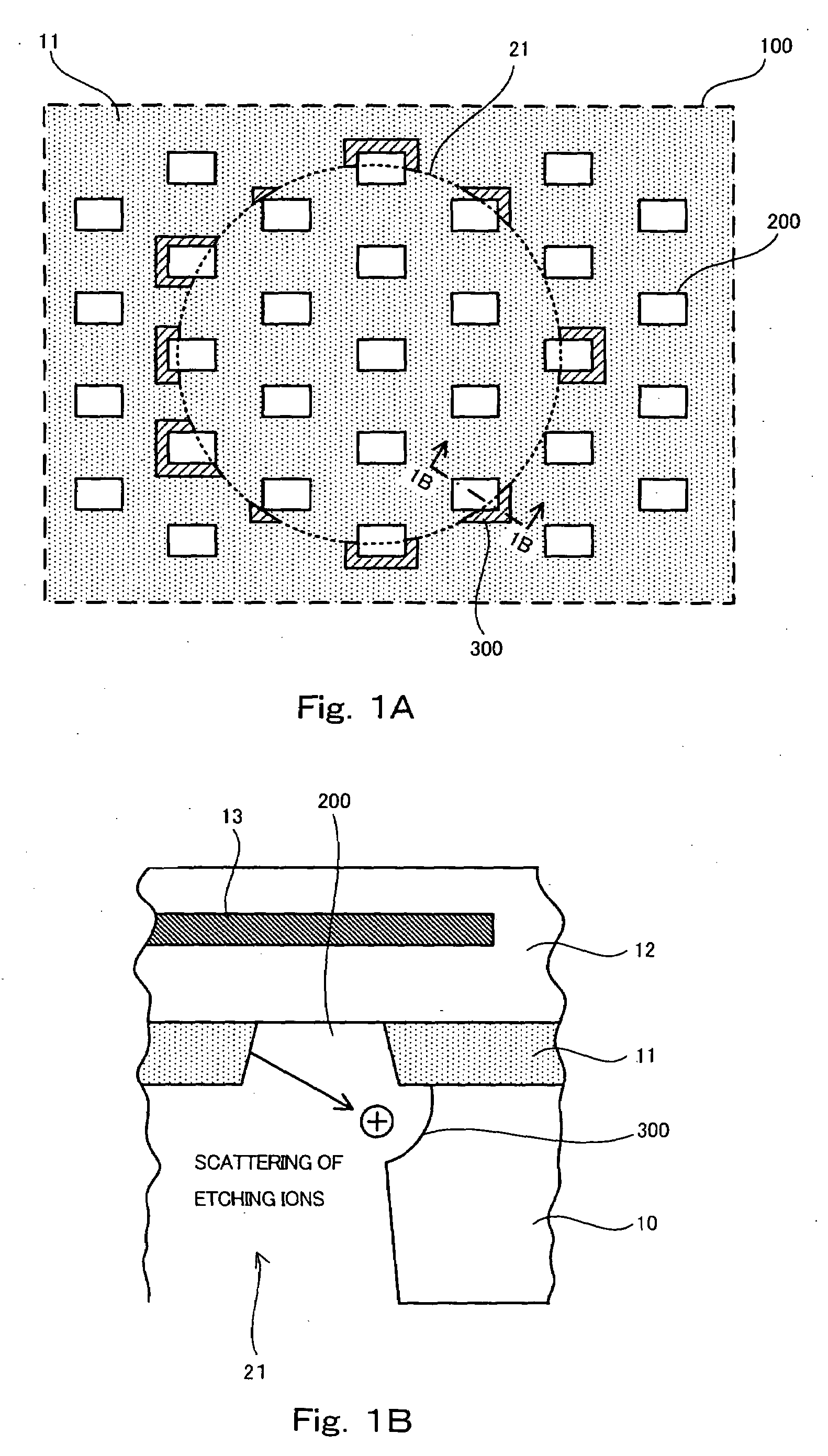
[0030]The supposed mechanism by which notches are generated in the side wall of a Through Silicon VIA hole when a Through Silicon VIA electrode is formed through a non-active area in which a plurality of dummy actives are uniformly disposed will be described with reference to FIGS. 1A and 1B before a description regarding embodiments of the present invention is given.

[0031]Notches in the sidewall of a Through Silicon VIA hole are known to be generated in the dry etching step of a semiconductor substrate when a Through Silicon VIA hole is formed. In the dry etching step, an STI region 11 composed of SiO2 is not etched by selective etching in the step for etching silicon as the base material of a semiconductor substrate 10. For this reason, the inventor posits that etching ions emitted by an etching device are reflected in the STI region 11, are scattered in the lateral direction, and collide with the sidewall of the Through Silicon VIA hole 21, whereby the sidewall of the Through Sil...


PUM


Abstract

There is provided a semiconductor device comprising a semiconductor substrate having an active area in which a plurality of active elements are formed, and a non-active area excepting the active area; at least one electrode pad electrically connected to any of the active elements. At least one Through Silicon VIA electrode is formed, being electrically connected to the electrode pad by way of the non-active area. The non-active area has an insulating region obtained by forming an insulating film on the semiconductor substrate, and a dummy section obtained by leaving a base material of the semiconductor substrate in the insulating region. The dummy section is provided in a position where an outer edge of the Through Silicon VIA electrode does not intersect with the boundary between the insulating region and the dummy section.

Description

BACKGROUND OF THE INVENTION[0001]1. Field of the Invention[0002]The present invention relates to a method for manufacturing a semiconductor device and a semiconductor package, and particularly relates to a semiconductor device having a Through Silicon VIA electrode structure.[0003]2. Description of the Related Art[0004]Recent versions of information devices such as digital cameras and mobile phones equipped with a camera function embody considerably higher levels of miniaturization, density, and functionality. A wafer-level chip size package (hereinafter referred to as W-CSP) is a known technique for reducing the size of CCD sensors, CMOS sensors, and other imaging elements used in such devices to fit in a chip-scale package.[0005]The W-CSP is a new concept package in which all the assembly steps are completed in a wafer state.[0006]A Through Silicon VIA electrode structure is adopted in the image sensor of a W-CSP structure because reliability can be improved and the device can be ...

Claims


Application Information

Patent Timeline
IPC IPC(8): H01L23/538H01L21/768
CPCH01L21/76898H01L23/481H01L2224/05H01L2224/0401H01L2224/05548H01L2224/13021H01L2224/13024H01L2224/02372H01L27/14636H01L21/31053H01L21/3212H01L21/76224H01L21/76229H01L21/76819H01L2225/06541
Inventor KOIKE, OSAMUKADOGAWA, YUTAKA
Owner TAIWAN SEMICON MFG CO LTD
Why Eureka
Try Eureka