

Method of producing semiconductor wafer
a technology of semiconductor material and manufacturing method, which is applied in the direction of semiconductor/solid-state device manufacturing, basic electric elements, electric apparatus, etc., can solve the problems of number of steps, loss of semiconductor material, etc., and achieves the effect of reducing the machining allowance of silicon material, and preventing cracking or chipping
Inactive Publication Date: 2010-01-14
SUMCO CORP
View PDF0 Cites 5 Cited by
- Summary
- Abstract
- Description
- Claims
- Application Information
AI Technical Summary
Benefits of technology
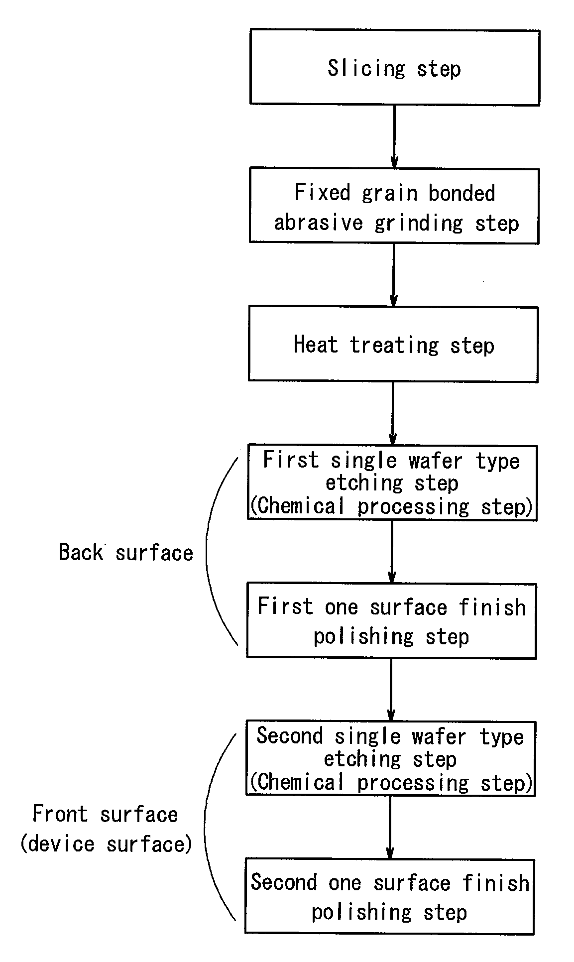
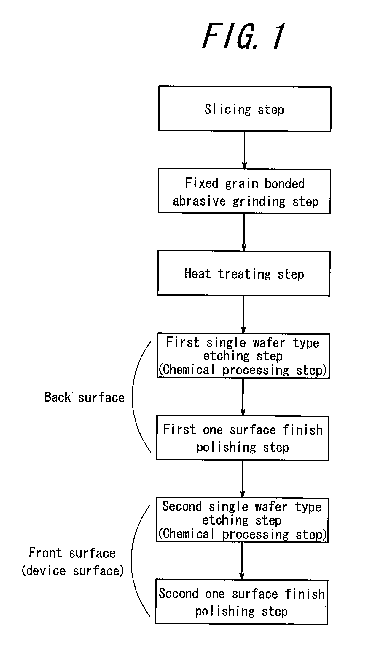
The invention provides a method for producing a semiconductor wafer that reduces the number of steps and machining allowance of the semiconductor wafer, resulting in a cheaper and more efficient production process. The method includes a slicing step, a fixed grain bonded abrasive grinding step, a heat treating step, and a one-side polishing step. By eliminating the need for a beveling step, the method reduces kerf loss and edge damage in the semiconductor wafer. Additionally, the method improves the flatness of the semiconductor wafer by reducing the machining allowance of the semiconductor wafer.
Problems solved by technology
The above-mentioned conventional method is a method for producing a double-side mirror-finished semiconductor wafer through the two beveling steps, lapping step and one-side grinding step, so that the number of steps is large and there is a problem that kerf loss of a semiconductor material (loss of a semiconductor material due to increase of lapping debris and one-side grinding debris) is caused.
Further, since the heat treatment is conducted lastly, there is a problem that strains generated in a semiconductor wafer by the heat treatment lead to cause cracking, chipping and the like through vibrations or impacts during the transportation or in the production of a semiconductor device.
Furthermore, when the aforementioned lapping step is included in the production method of a silicon wafer having a diameter of not less than 450 mm, there is a fear that the lapping apparatus significantly grows in size and problems occur with respect to installation site of the lapping apparatus or the like in the formulation of a production line.
Furthermore, as thermal stress is increased with the increase of the diameter in the large-size wafer, there is a problem that strains generated in the heat treatment lead to cause cracking, chipping and the like through vibrations or impacts during the transportation or in the production of a semiconductor device.
Method used
View moreImage
Smart ImageViewing Examples

Examples
example 1
[0096]A sample silicon wafer having a diameter of 300 mm is prepared according to the process flow of an embodiment of the invention shown in FIG. 1.
example 2
[0097]A sample silicon wafer is prepared by the same production method as in Example 1 except that the diameter of the silicon wafer is 450 mm.
Login to View More PUM
 Abstract
There is provided a production method in which the beveling step conducted for preventing the cracking or chipping in a raw wafer during the grinding can be omitted when the raw wafer cut out from a crystalline ingot is processed into a double-side mirror-finished semiconductor wafer and a semiconductor wafer can be obtained cheaply by shortening the whole of the production steps for the semiconductor wafer and decreasing the machining allowance of silicon material in the semiconductor wafer to reduce the kerf loss of the semiconductor material as compared with the conventional method.The method is characterized by comprising a slicing step of cutting out a thin disc-shaped raw wafer from a crystalline ingot; a fixed grain bonded abrasive grinding step of sandwiching the raw wafer between a pair of upper and lower platens each having a pad of fixed grain bonded abrasive to simultaneously grind both surfaces of the raw wafer; a heat treating step of subjecting the raw wafer to a given heat treatment after the fixed grain bonded abrasive grinding step; and a one-side polishing step of polishing each of the both surfaces of the raw wafer after the heat treating step.
Description
BACKGROUND OF THE INVENTION[0001]1. Field of the Invention[0002]This invention relates to a method of producing a semiconductor wafer and, more particularly to a method of producing a double-side mirror-finished semiconductor wafer by cutting out a thin disc-shaped raw wafer from a crystalline ingot.[0003]2. Description of the Related Art[0004]In general, the conventional method of producing a semiconductor wafer comprises sequentially-conducted steps of (Slicing step)→(First beveling step)→(Lapping step)→(Second beveling step)→(One-side grinding step)→(Double-side polishing step)→(One-side finish polishing step)→(Heat treatment).[0005]In the slicing step, a thin disc-shaped raw wafer is cut out from a crystalline ingot by cutting. In the first beveling step, an outer peripheral portion of the cut raw wafer is beveled so as to suppress chipping or cracking of the raw wafer in the subsequent lapping step. In the lapping step, the beveled raw wafer is lapped, for example, with a grind...
Claims
Login to View More Application Information
Patent Timeline
 Patent Type & AuthorityApplications(United States)
IPC IPC(8): H01L21/322
CPCH01L21/3225H01L21/02008Y02P80/30
InventorSHIOTA, TAKAAKIITOU, WATARUNAKAYAMA, TAKASHI
OwnerSUMCO CORP