Semiconductor device, production method for the same, and substrate

a semiconductor device and production method technology, applied in the direction of manufacturing tools, welding/cutting media/materials, welding apparatus, etc., can solve the problems of reducing the bonding strength between the semiconductor chip and the wiring board, cracking from and the formation of the au—sn alloy layer is not perfectly prevented by the reduction of the thickness, so as to achieve the effect of ensuring cracking and high bonding strength

Active Publication Date: 2010-01-21
ROHM CO LTD
View PDF8 Cites 10 Cited by
  • Summary
  • Abstract
  • Description
  • Claims
  • Application Information

AI Technical Summary

Benefits of technology

[0017]According to this production method, an Au—Sn—Ni alloy layer is formed as having undulations in an interface between the Au—Sn—Ni alloy layer and the solder layer, and an Au—Sn alloy phase is dispersed in the solder layer. This makes it p...

Problems solved by technology

When the semiconductor chip is soldered on such a wiring board, however, an Au—Sn alloy layer is formed from Au of the Au layer and Sn of a solder in an interface between the Au layer and the solder, thereby reducing the bonding strength between the semiconductor chip and the wiring board.
This causes a problem that cracking occurs from the Au—Sn alloy layer due to heat shock, heat cycle and the like.
However, the formation of the Au—Sn alloy layer is not perfectly prevented by the reductio...

Method used


Image

  • Semiconductor device, production method for the same, and substrate
  • Semiconductor device, production method for the same, and substrate
  • Semiconductor device, production method for the same, and substrate

Examples


Embodiment Construction

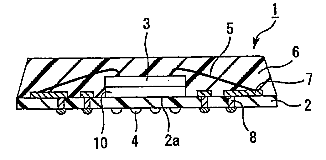
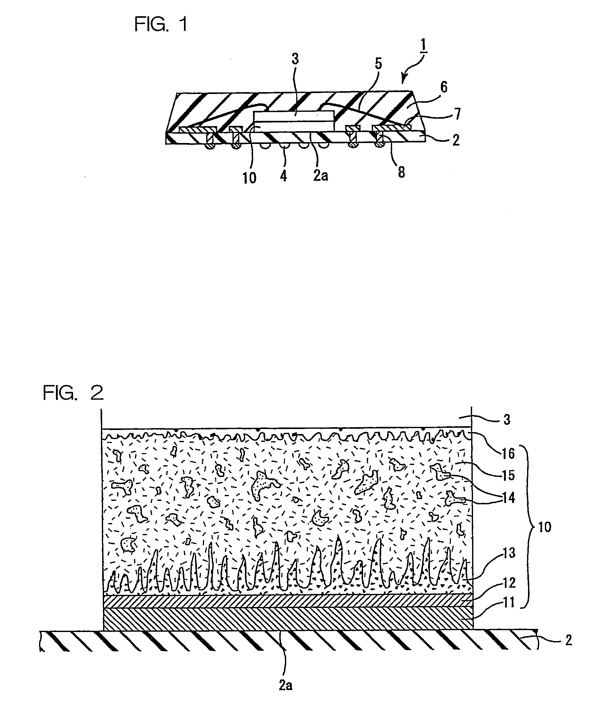
[0023]FIG. 1 is a sectional view schematically illustrating a semiconductor device according to one embodiment of the present invention. The semiconductor device 1 includes a substrate 2 of a glass fiber reinforced resin. On a front surface of the substrate 2, a conductor circuit 7 having a laminate structure including a Cu layer, an Ni layer and an Au layer stacked in this order is provided in an area other than a bonding area 2a to which a semiconductor chip 3 is bonded.

[0024]The glass fiber reinforced resin is not particularly limited, but examples thereof include an epoxy resin, a bismaleimide-triazine resin (BT resin), a polyester resin, a polyimide resin, a phenol resin and materials prepared by impregnating reinforcement materials such as glass fibers with these resins.

[0025]Solder bumps 4 are provided on a rear surface of the substrate 2. The solder bumps 4 are electrically connected to the conductor circuit 7 via through-holes 8. This embodiment is directed to a case in whi...


PUM

PropertyMeasurementUnit
Thicknessaaaaaaaaaa
Lengthaaaaaaaaaa

Abstract

A semiconductor device is provided in which a semiconductor chip is bonded to a substrate with a sufficiently increased bonding strength and cracking is assuredly prevented which may otherwise occur due to heat shock, heat cycle and the like. The semiconductor device includes a semiconductor chip and a substrate having a bonding area to which the semiconductor chip is bonded via a metal layer. The metal layer includes an Au—Sn—Ni alloy layer and a solder layer provided on the Au—Sn—Ni alloy layer. Undulations are formed in an interface between the Au—Sn—Ni alloy layer and the solder layer.

Description

TECHNICAL FIELD[0001]The present invention relates to a semiconductor device, a production method for the semiconductor device, and a substrate to be used for the semiconductor device.BACKGROUND ART[0002]Conventionally, there exist semiconductor devices which are produced by soldering a semiconductor chip such as an LSI chip on a wiring board having an Au layer formed on a surface thereof and sealing the chip and the board with a resin. The Au layer on the surface of the wiring board is formed by plating or sputtering in order to ensure solder wettability and prevent oxidation of interconnections. When the semiconductor chip is soldered on such a wiring board, however, an Au—Sn alloy layer is formed from Au of the Au layer and Sn of a solder in an interface between the Au layer and the solder, thereby reducing the bonding strength between the semiconductor chip and the wiring board. This causes a problem that cracking occurs from the Au—Sn alloy layer due to heat shock, heat cycle a...

Claims


Application Information

Patent Timeline
IPC IPC(8): H01L23/488H01L21/60B23K31/02
CPCH01L23/49811H01L2924/00013H01L24/29H01L24/48H01L24/83H01L2224/04026H01L2224/29144H01L2224/32225H01L2224/32507H01L2224/48091H01L2224/48227H01L2224/73265H01L2224/83801H01L2924/01004H01L2924/01005H01L2924/01015H01L2924/01029H01L2924/01033H01L2924/01047H01L2924/0105H01L2924/01051H01L2924/01058H01L2924/01078H01L2924/01079H01L2924/01082H01L2924/14H01L2924/1433H01L2924/15311H01L2924/0132H01L2924/0133H01L24/32H01L2224/29H01L2224/2919H01L2224/29298H01L2924/01006H01L2924/014H01L2924/0665H01L2224/29101H01L2224/83444H01L2924/0134H01L2224/29109H01L2224/29111H01L2924/15788H01L23/49866H01L2924/00014H01L2924/00H01L2924/01028H01L2924/00012H01L2924/01049H01L2924/01083H01L2924/3512H01L2224/29099H01L2224/29199H01L2224/29299H01L2224/2929H01L2224/451H01L24/73H01L2924/181H01L2224/45099H01L2224/05599H01L21/52H01L25/00B23K35/26
Inventor HADA, MOTOHARUKASUYA, YASUMASAMATSUBARA, HIROAKI
Owner ROHM CO LTD
Why Eureka
Try Eureka