
Precharge and evaluation phase circuits for sense amplifiers

a technology of phase circuit and amplifier, which is applied in the direction of digital storage, static storage, instruments, etc., can solve the problems of inverter but being usually more complex, the evaluation node is very slow during evaluation, and the sense operation could fail, so as to reduce the die area of sense circuit, optimize the characteristics of each circuit, and increase read performance

Active Publication Date: 2010-01-21
ATMEL CORP
View PDF38 Cites 3 Cited by
  • Summary
  • Abstract
  • Description
  • Claims
  • Application Information

AI Technical Summary

Benefits of technology

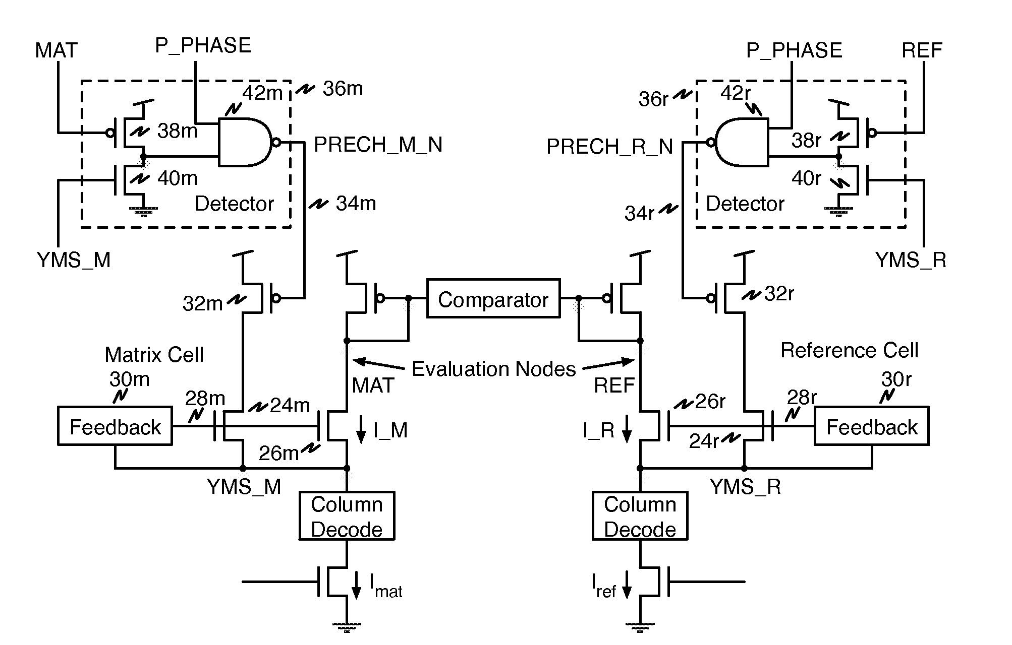
[0031]According to the present invention, better control of the precharge and evaluation phases is exerted, allowing the use of significantly smaller transistors, thus reducing sense-circuit die area and increasing read performance.
[0032]According to the present invention, the sense-amplifier circuitry is split such that a part of circuitry is principally used / optimized for high currents (in particular the precharge phase) and another part is principally used / optimized for low currents (in particular the evaluation phase). In this way it is possible to optimize the characteristics of each circuit, minimize area, speed up access time, allowing all transistors to work in their best polarization point. The approach of the present invention is useful for sense amplifiers generally and not only for the one disclosed herein. The concept of the present invention may be applied to any kind of sense amplifier.
[0033]Moreover even if involved currents may be significantly different according to the sense architecture and to the kind of flash memory this approach can be, in any case, easily adapted and optimized, that is, for example one part may be optimized for high / medium currents and the other one for low / medium currents or the different optimized parts can be several, one optimized for high current, another for medium currents another for low currents, any combination of these kinds of circuitry can be easily obtained.

Problems solved by technology

This presents another drawback due to their dimensions and their terminal capacitance, making the evaluation nodes very slow during evaluation mode where the currents are very low.
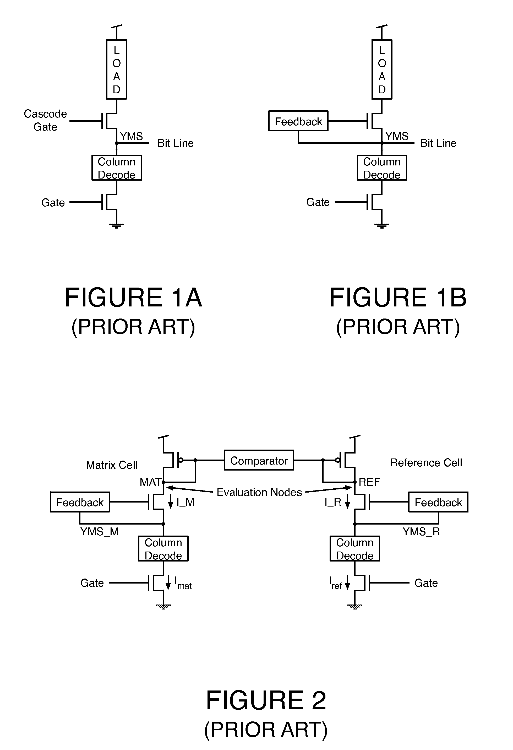
The most simple feedback circuitry may be an inverter but is usually more complex.
If transient (i.e., capacitive) currents are not negligible during the evaluation phase these current relationships may not be true and the sense operation could fail.
This time often is not acceptable when a fast access time is required.
For these reasons they are very large and have high gate capacitance.
This slows the sense process, because the currents Imat, and Iref are very low and take a significant amount of time to move the voltages at these high-capacitance evaluation nodes.
This is particularly critical especially during the last part of the precharge phase, that for this reason can take a long time.
Moreover, the matrix and reference cascode transistors need to be very large because they also have to be able, for the same reasons, to furnish a very high current to quickly complete the precharge phase.
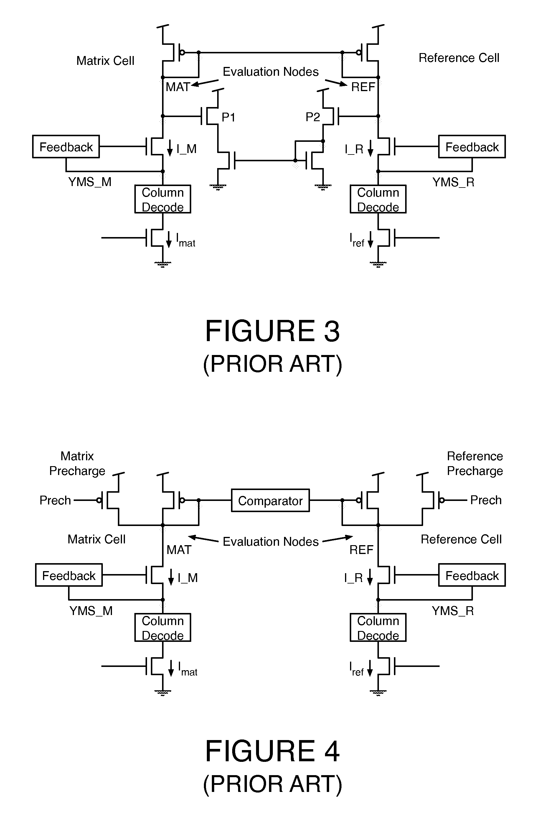
The solution shown in FIG. 4 speeds up the precharge phase but has the drawback that there is a significant risk that the evaluation nodes are biased at values that are too high with respect the target values at the end of the precharge phase.
It is very difficult to find the correct duration of this new phase to avoid this problem.
Since only low currents flow during the evaluation phase, the evaluation nodes still need to be discharged to the correct values after the precharge phase, a finite time is needed and a sensing error can thus occur.
Other parallel precharge solutions using transistors having different thresholds have been proposed to avoid this risk, but such solutions are not efficient enough to allow significant reduction of the sizes of the p-channel diode-connected transistors and to reduce access time.

Method used


Image

  • Precharge and evaluation phase circuits for sense amplifiers
  • Precharge and evaluation phase circuits for sense amplifiers
  • Precharge and evaluation phase circuits for sense amplifiers

Examples


Embodiment Construction

[0048]Persons of ordinary skill in the art will realize that the following description of the present invention is illustrative only and not in any way limiting. Other embodiments of the invention will readily suggest themselves to such skilled persons.

[0049]The overall goal is to increase speed / performance and to significantly reduce the die area of the sense amplifier while being careful to avoid over biasing the evaluation nodes (MAT, REF) and the cascode feedback inputs YMS_M, YMS_R and being able to get them very close to their correct values at the end of precharge phase. A sense amplifier according to the present invention includes minimized / optimized precharge circuitry that is able to quickly precharge the bitlines with minimized / optimized precharge circuitry, must minimize / optimize the evaluation p-channel transistors, must minimize / optimize the comparator transistors of both polarities, and also minimizes / optimizes cascode transistors. An important target is to obtain the...


PUM


Abstract

A precharge and evaluation circuit for a memory sense amplifier includes a first precharge-phase transistor having a source coupled to a power-supply potential, a gate coupled to a precharge control line, and a drain. A second precharge-phase transistor has a drain coupled to the drain of the first precharge-phase transistor, a source, and a gate coupled to the source through a feedback circuit. A first read-phase transistor has a source coupled to the power-supply potential, and a gate and drain coupled to a comparator. A second read-phase transistor has a drain coupled to the drain of the first read-phase transistor, a source coupled to the source of the second precharge-phase transistor, and a gate coupled to the source of the second read-phase transistor through a feedback circuit. A column decoder is coupled to the sources of the second precharge-phase and second read-phase transistors.

Description

BACKGROUND OF THE INVENTION[0001]1. Field of the Invention[0002]The present invention relates to precharge and evaluation circuits for memory sense amplifiers.[0003]2. Related Art[0004]In order to correctly read the data item from a memory cell of a memory matrix, it is customary to compare the current read from the memory matrix cell with the current read from a reference matrix cell or with a reference current, in order to detect the difference between a programmed cell and an erased cell.[0005]For this purpose, memory matrices are usually configured so that reading data from a memory cell is performed by comparing a current that flows across a reference matrix cell (or a reference current) with the current of the selected cell. The difference between the two currents determines the value of the data. If the matrix cell current is higher than reference current then the stored data is a “one” bit; otherwise it is a zero bit.[0006]To get the correct current flowing the selected cell...

Claims


Application Information

Patent Timeline
IPC IPC(8): G11C7/00
CPCG11C7/08G11C16/28G11C7/12
Inventor BEDARIDA, LORENZOTASSAN CASER, FABIOCHINOSI, MAUROFERRARIO, DONATO
Owner ATMEL CORP
Learn More