Etched-facet ridge lasers with etch-stop

a laser device and etch-stop technology, applied in the field of etched-facet photonic devices, can solve the problems of difficult precision control and incomplete design of dry etch steps, and achieve the effects of improving the manufacturing process, high uniformity and yield, and increasing the yield of the fabrication process

Active Publication Date: 2010-01-21
MACOM TECH SOLUTIONS HLDG INC
View PDF2 Cites 9 Cited by
  • Summary
  • Abstract
  • Description
  • Claims
  • Application Information

AI Technical Summary

Benefits of technology

[0006]Since high uniformity and yield for etched facet ridge devices is extremely desirable, an improved process for fabricating an etched-facet ridge laser device is provided in accordance with the present invention. In this process, a ridge laser having etched facets is formed in an epitaxial structure that incorporates a wet etch stop layer at the location where the base of the ridge is to be located. The ridge is partially formed using a prior art lithography and dry etch process, but the dry etch is stopped short of the ridge base. Lithography defines a wet etch window that overlaps the partially etched ridge while keeping its end sections and its end facets protected by a resist layer. Then the structure is wet-etched to complete the formation of the ridge and to remove residual material from above the etch stop layer. The stop layer in the epitaxial structure precisely and reliably stops the wet etch at the depth desired for the base of the ridge structure, increasing the yield of the fabrication process to about 98-99.8%.
[0008]In accordance with the present invention, a wet etch stop layer is epitaxially deposited on the substrate at the level of the base of the ridge that is to be formed in the structure. Thus, for example, a stop layer of Gallium Indium Arsenide Phosphide (GaInAsP) is deposited in the cap layer, just above the upper cladding layer. This stop layer is about 20 nm thick, and is lattice matched with the InP cladding layer. The resulting wafer is processed using standard photolithography and chemically assisted ion beam etching (CAIBE) dry etching steps to form one or more laser cavities and facets. Thereafter, a second photolithography step is used to define one or more ridges on the previously formed cavities, and CAIBE is used to etch the ridges. Since the CAIBE process is hard to control with precision, and thus is not very accurate, this dry etch step is designed to be incomplete; i.e., it is designed to end short of the desired depth of the ridge and before it reaches the stop layer. Thereafter, another photolithography step is performed to cover the end sections of the ridge and the facets with a protective resist layer and a wet etch step, using a selective wet etchant, is performed. The selective wet etchant, for example a mixture of HCl and H3PO4, removes the residual upper cladding material and stops on or etches only very slowly, the etch stop layer. Thus, the wet etch completes the ridge formation and stops at the stop layer. Although it etches laterally a small amount at the bottom of the ridge, this is easily accounted for, and the process serves to form a ridge having precisely the desired dimensions. This wet etch also removes any residual artifacts left by the dry etch step, and produces a ridge structure having a high degree of precision, resulting in a high device yield.

Problems solved by technology

Since the CAIBE process is hard to control with precision, and thus is not very accurate, this dry etch step is designed to be incomplete; i.e., it is designed to end short of the desired depth of the ridge and before it reaches the stop layer.

Method used


Image

  • Etched-facet ridge lasers with etch-stop
  • Etched-facet ridge lasers with etch-stop
  • Etched-facet ridge lasers with etch-stop

Examples


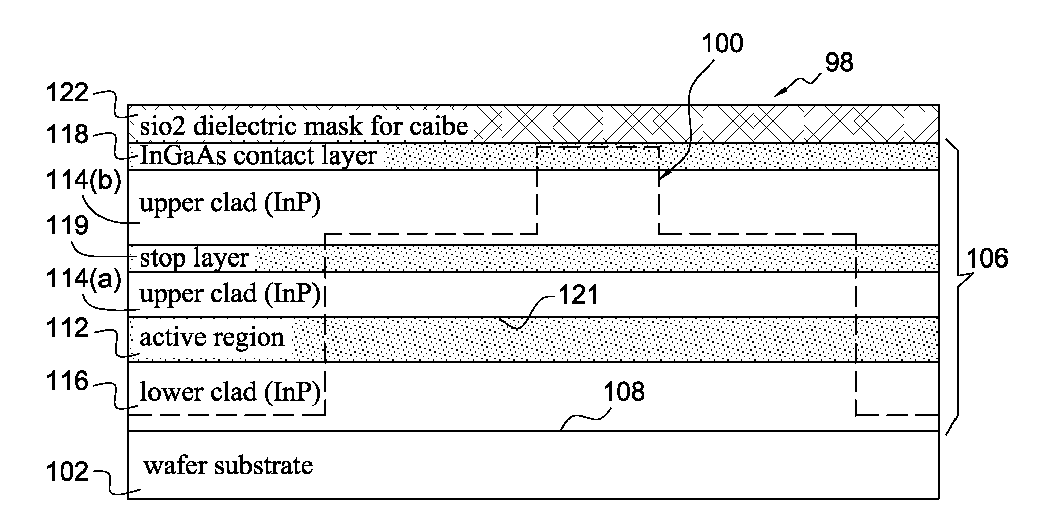
Embodiment Construction

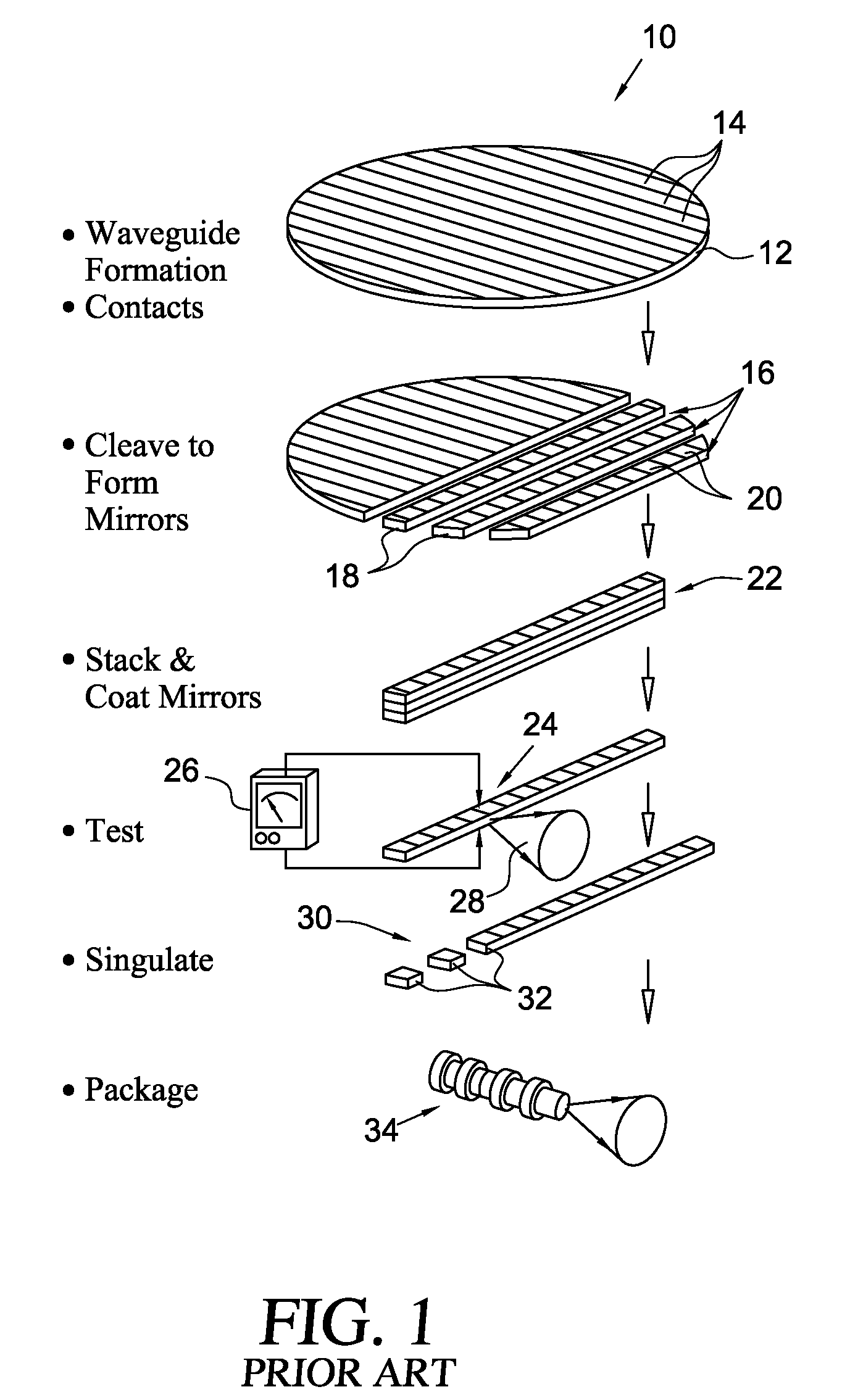
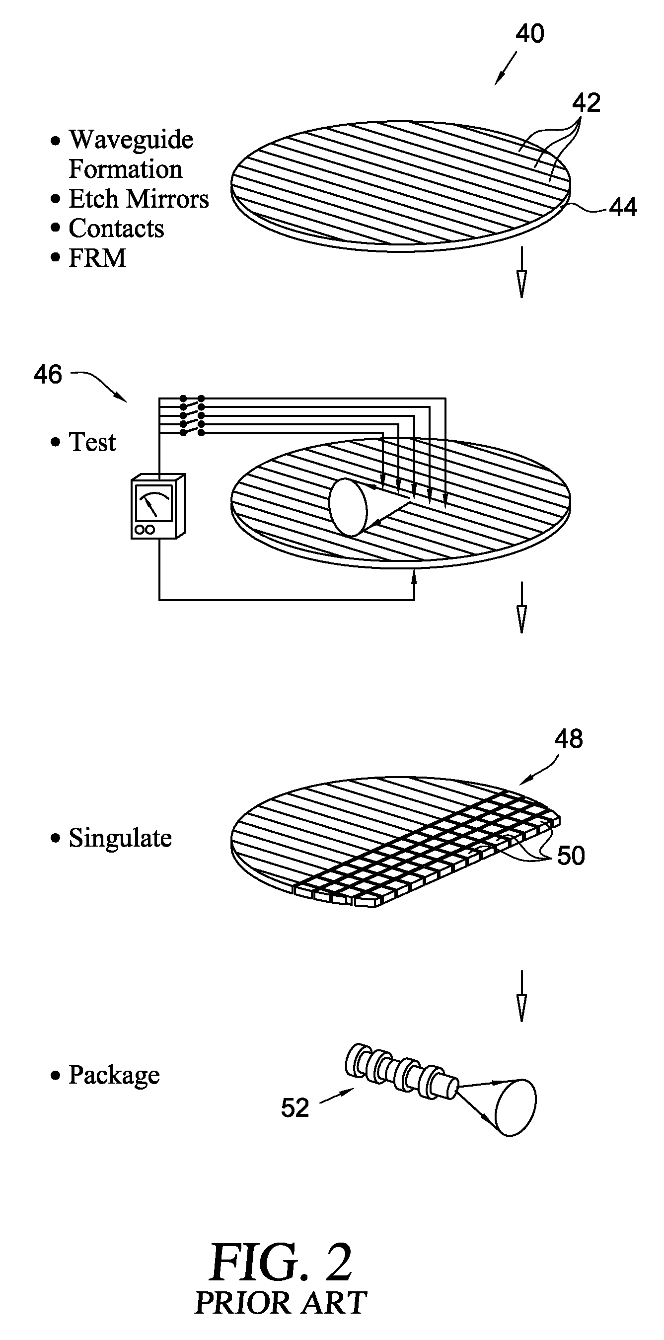
[0017]As generally illustrated at 10 in FIG. 1, mechanical cleaving of a semiconductor epi wafer 12 is the usual process for defining reflective mirrors, or facets, at the cavity ends of edge-emitting diode lasers, fabricated on the wafer. In this process, multiple waveguides 14 are fabricated on the wafer substrate, a metal contact layer is applied, and the wafer is mechanically cleaved, as along cleave lines 16, to form bars 18 of laser devices 20. The bars 18 are then stacked, as illustrated at 22, and the cleaved end facets of the laser devices are coated to provide the desired reflection and emission characteristics. The individual laser devices 20 may then be tested, as at 24, by applying a bias voltage 26 across the individual lasers and detecting the resulting output light beam 28. The bars of laser devices may then be separated, or singulated, as at 30, to produce individual chips 32 each containing one or more laser devices that may be suitably packaged, in known manner, a...


PUM


Abstract

A photonic device incorporates an epitaxial structure having an active region, and which includes a wet etch stop layer above, but close to, the active region. An etched-facet ridge laser is fabricated on the epitaxial structure by dry etching followed by wet etching. The dry etch is designed to stop before reading the depth needed to form the ridge. The wet etch completes the formation of the ridge and stops at the wet etch stop layer.

Description

CROSS REFERENCE TO RELATED APPLICATIONS[0001]This application is a Divisional of copending U.S. application Ser. No. 11 / 644,828, filed on Dec. 26, 2006.FIELD OF THE INVENTION[0002]The present invention relates, in general, to etched-facet photonic devices, and more particularly to improved etched-facet ridge laser devices of the type disclosed in copending U.S. application Ser. No. 11 / 356,203, filed on Feb. 17, 2006 and entitled “High Reliability Etched Facet Photonic Devices” (Attorney's Docket BIN 20) and assigned to the assignee of the present application, and to a process for fabricating such devices.BACKGROUND OF THE INVENTION[0003]Semiconductor lasers typically are fabricated on a wafer by growing an appropriate layered semiconductor material on a substrate through Metalorganic Chemical Vapor Deposition (MOCVD) or Molecular Beam Epitaxy (MBE) to form an epitaxy structure having an active layer parallel to the substrate surface. The wafer is then processed with a variety of sem...

Claims


Application Information

Patent Timeline
Patent Type & Authority Applications(United States)
IPC IPC(8): H01L21/30
CPCH01S5/209H01S5/2214H01S5/22
Inventor BEHFAR, ALEX A.SCHREMER, ALFRED T.STAGARESCU, CRISTIAN B.
Owner MACOM TECH SOLUTIONS HLDG INC
Why Eureka
Try Eureka