
Etched-facet ridge lasers with etch-stop
a technology of etched facets and lasers, which is applied in the direction of lasers, laser construction details, semiconductor lasers, etc., can solve the problems of difficult precision control and incomplete design of dry etch steps, and achieve the improvement of the process for fabricating, high uniformity and yield, and the effect of increasing the yield of the fabrication process
- Summary
- Abstract
- Description
- Claims
- Application Information
AI Technical Summary
Benefits of technology
Problems solved by technology
Method used
Image

Examples
Embodiment Construction
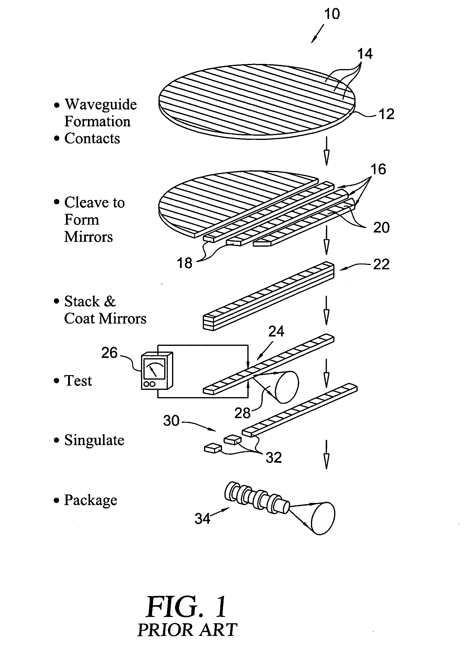
[0016]As generally illustrated at 10 in FIG. 1, mechanical cleaving of a semiconductor epi wafer 12 is the usual process for defining reflective mirrors, or facets, at the cavity ends of edge-emitting diode lasers, fabricated on the wafer. In this process, multiple waveguides 14 are fabricated on the wafer substrate, a metal contact layer is applied, and the wafer is mechanically cleaved, as along cleave lines 16, to form bars 18 of laser devices 20. The bars 18 are then stacked, as illustrated at 22, and the cleaved end facets of the laser devices are coated to provide the desired reflection and emission characteristics. The individual laser devices 20 may then be tested, as at 24, by applying a bias voltage 26 across the individual lasers and detecting the resulting output light beam 28. The bars of laser devices may then be separated, or singulated, as at 30, to produce individual chips 32 each containing one or more laser devices that may be suitably packaged, in known manner, a...
PUM
 Abstract
Description
Claims
Application Information