Non-volatile memory storage system with two-stage controller architecture
- Summary
- Abstract
- Description
- Claims
- Application Information
AI Technical Summary
Benefits of technology
Problems solved by technology
Method used
Image
Examples
Embodiment Construction
[0043]The present invention will now be described in detail with reference to preferred embodiments thereof as illustrated in the accompanying drawings.
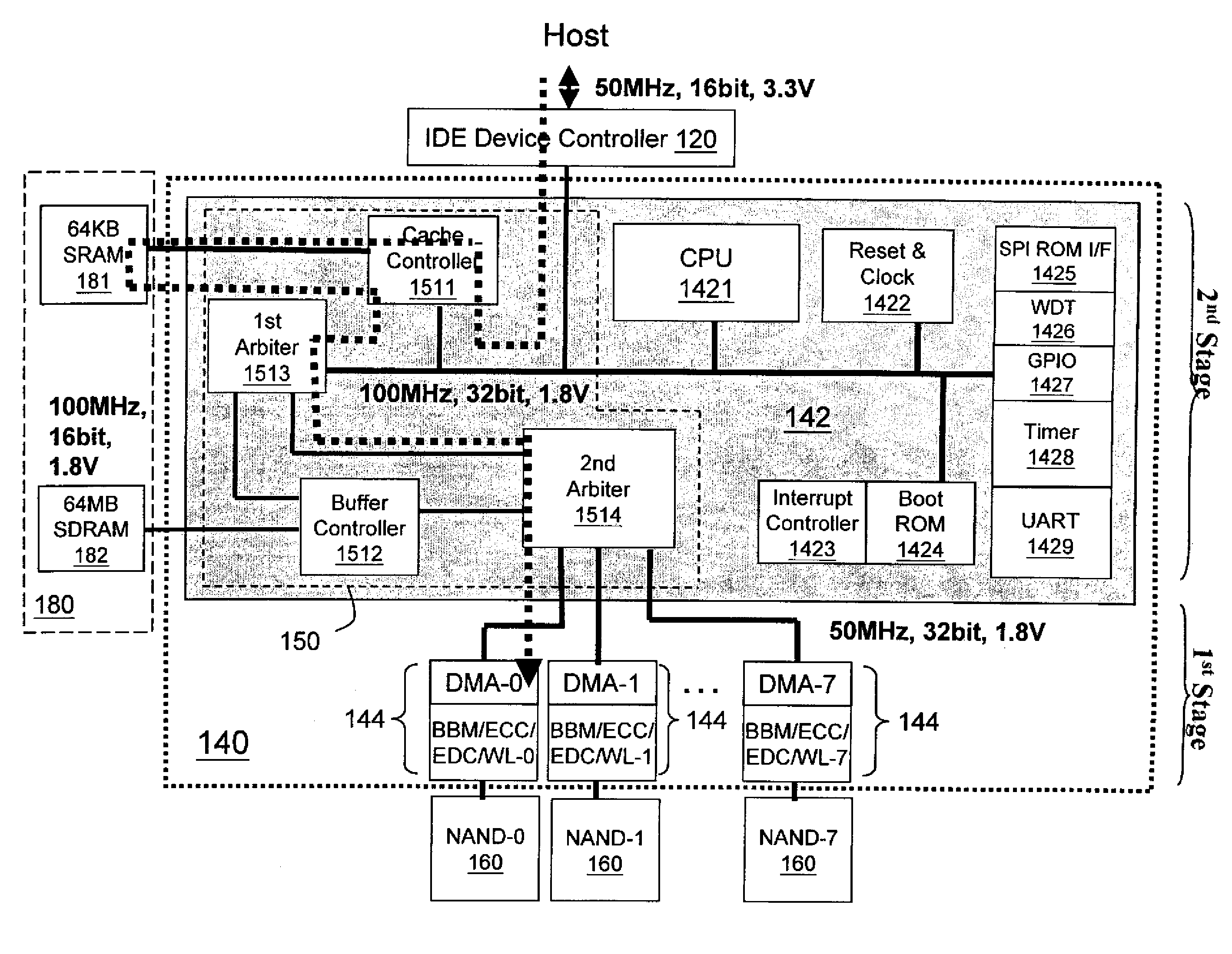
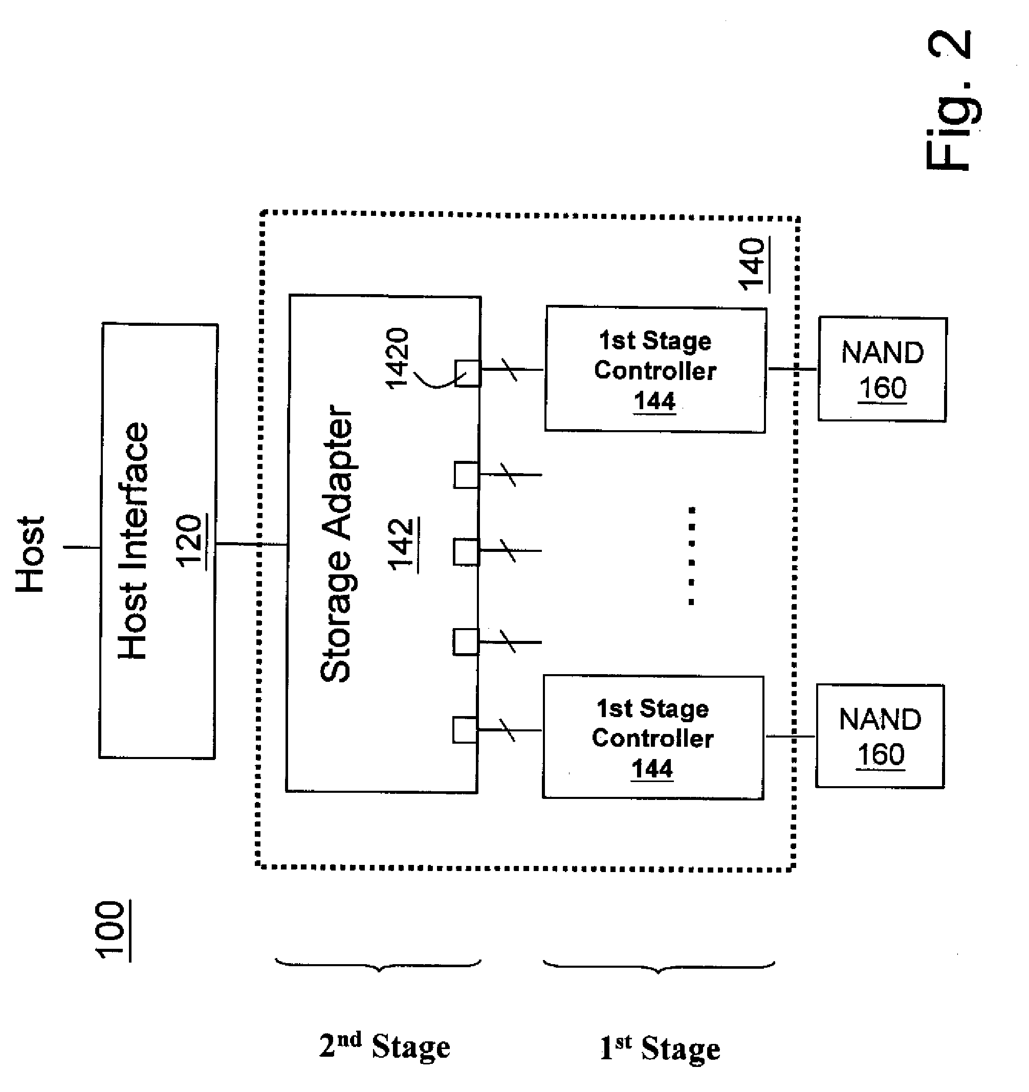
[0044]The first embodiment of the present invention is shown in FIG. 2. The solid state data storage system 100 employs two-stage controller architecture. As shown in the figure, the system 100 includes a host interface 120 for communication between the system 100 and a host; a two-stage controller 140 including a storage adapter 142 and a plurality of first stage controllers 144; and a plurality of non-volatile memory devices 160, such as NAND flash devices as shown but can be other types of NVM devices such as SONOS or CTF (Charge Trapping Flash). The host interface 120 may communicate with the host through, e.g., IDE, SATA, USB, PCI or PCIe protocol. The storage adapter 142 has a plurality of internal interfaces 1420, and it may communicate with the plurality of first stage controllers 144 through any designated protocol, such as ...
PUM
 Abstract
Description
Claims
Application Information


