Solar cell and manufacturing method thereof

a technology of solar cells and manufacturing methods, applied in printing presses, semiconductor devices, printing, etc., can solve the problem of more likely problems, achieve the effect of reducing the amount of conductive materials pushed, reducing the risk of problems, and increasing the printing speed

Active Publication Date: 2010-01-28
PANASONIC INTELLECTUAL PROPERTY MANAGEMENT CO LTD
View PDF4 Cites 34 Cited by
  • Summary
  • Abstract
  • Description
  • Claims
  • Application Information

AI Technical Summary

Benefits of technology

[0042]According to the method of manufacturing a solar cell 10 of the embodiment, first printing speed VI at which first conductive material 31S is printed is faster than second printing speed V2 at which second conductive material 32S is printed.
[0043]FIG. 6 shows the relationship between first printing speed V1 and the line-width of first conductive layer 31, and also the relationship between second printing speed V2 and the line-width of second conductive layer 32. Note that the values on the vertical axis of the graph shown in FIG. 6 are normalized values with the line-width of first conductive layer 31 formed at a speed of 50 mm/sec being 1.
[0044]FIG. 6 shows that the line-widths of conductive layers 31 and 32 tend to be narrower as their respective printing speeds V1 and V2 increase. This is because the faster the printing speed becomes, the smaller the amount of the conductive material pushed out of screen plate 51 becomes.
[0045]In addition, the line-width of second conductive layer 32 tends to become narrower than the line-width of first conductive layer 31 for the following reason. The texture formed in the surface of photoelectric co...

Problems solved by technology

This problem is more likely to occur when a plurality of bumps are formed on the surface of the pho...

Method used


Image

  • Solar cell and manufacturing method thereof
  • Solar cell and manufacturing method thereof
  • Solar cell and manufacturing method thereof

Examples


examples

[0055]What follows is a specific description of various examples of the solar cell according to the invention, but the examples given below are not the only ones of the invention. The invention can be carried out in various appropriately modified forms as long as the gist of the invention is kept intact.

(Fabrication of Solar Cells)

[0056]Solar cells of Comparative Examples and Examples of the invention are fabricated in the following way.

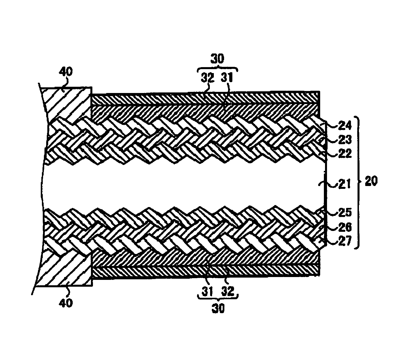
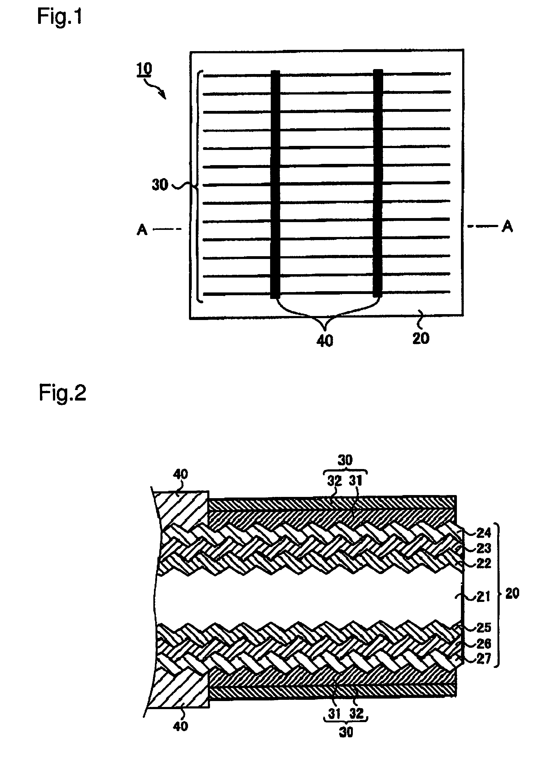
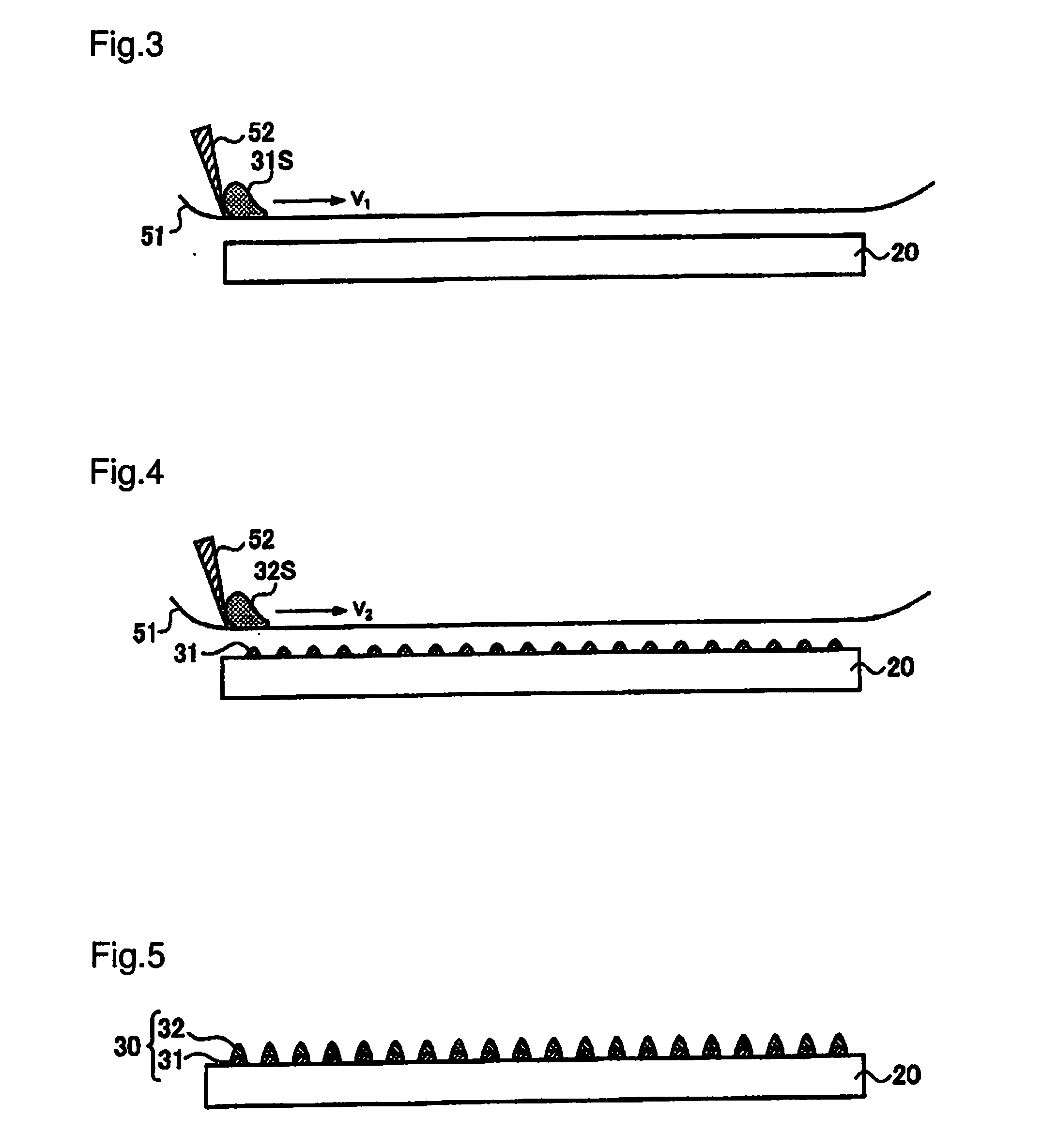
[0057]To begin with, an anisotropic etching process is performed on n type monocrystalline silicon wafers each 104 millimeters square, so that a plurality of bumps (texture) are formed on the surface of the n type monocrystalline silicon wafers.

[0058]Subsequently, on a first main surface of each n type monocrystalline silicon wafer, an i type amorphous silicon layer of an approximately 10-nm thickness and a p type amorphous silicon layer of an approximately 10-nm thickness are formed consecutively one upon the other by the plasma CVD method. Then, on...


PUM


Abstract

Provided is a solar-cell manufacturing method that is capable of preventing a conductive paste from bleeding and spreading on a photoelectric conversion body. In the provided method of manufacturing a solar cell, a first printing speed at which a first conductive material is printed is faster than a second printing speed at which a second conductive material is printed on the first conductive material.

Description

CROSS REFERENCE TO RELATED APPLICATIONS[0001]This application claims priority based on 35 USC 119 from prior Japanese Patent Application No. P2008-192701 filed on Jul. 25, 2008, entitled “Manufacturing Method of Solar Cell”, the entire contents of which are incorporated herein by reference.BACKGROUND OF THE INVENTION[0002]1. Field of the Invention[0003]The invention relates to a solar cell and method of manufacturing a solar cell including a plurality of fine line-shaped electrodes that are formed on a photoelectric conversion body.[0004]2. Description of Related Art[0005]Sunlight energy is a clean energy and can be supplied inexhaustibly. Solar cells are capable of converting sunlight energy directly into electric energy, and hence are expected to provide a new energy source from sunlight.[0006]A typical solar cell includes: a photoelectric conversion body configured to receive light and thus generate photogenerated carriers; and a plurality of fine line electrodes configured to co...

Claims


Application Information

Patent Timeline
IPC IPC(8): H01L31/00H01L31/18
CPCH01L31/022425Y02E10/50H01L31/0747B41F15/44H01L31/0224H01L31/18
Inventor NISHIWAKI, TAKESHIYOSHIMINE, YUKIHIRO
Owner PANASONIC INTELLECTUAL PROPERTY MANAGEMENT CO LTD
Why Eureka
Try Eureka