Organic electroluminescence device, process of producing organic electroluminescence device, and electronic apparatus

a technology of electroluminescence device and electroluminescence device, which is applied in the direction of discharge tube luminescnet screen, discharge tube/lamp details, coating, etc., can solve the problems of low flexibility and high young's modulus of film, and achieve long product life and high endurance

Active Publication Date: 2010-01-28
SEIKO EPSON CORP
View PDF7 Cites 65 Cited by
  • Summary
  • Abstract
  • Description
  • Claims
  • Application Information

AI Technical Summary

Benefits of technology

[0010]An advantage of some aspects of the invention is to provide an organic EL device exhibiting high reliability by being provided with a sealing layer having high endurance. Another advantage of some aspects of the invention is to provide a process of producing such an organic EL device. Further another advantage is to provide an electronic apparatus including such an organic EL device.

Problems solved by technology

Consequently, the film has a high density and a high gas barrier property, but, at the same time, the film has a high Young's modulus and is lack of flexibility.

Method used


Image

  • Organic electroluminescence device, process of producing organic electroluminescence device, and electronic apparatus
  • Organic electroluminescence device, process of producing organic electroluminescence device, and electronic apparatus
  • Organic electroluminescence device, process of producing organic electroluminescence device, and electronic apparatus

Examples


first embodiment

A First Embodiment

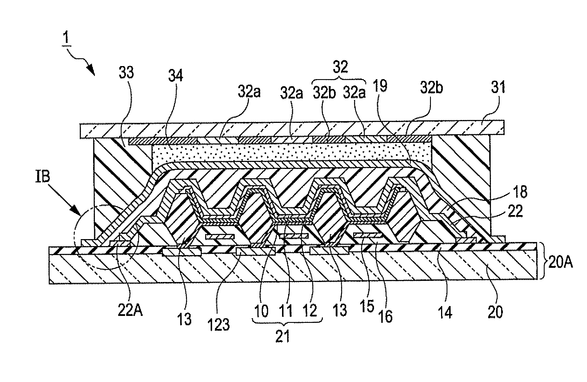
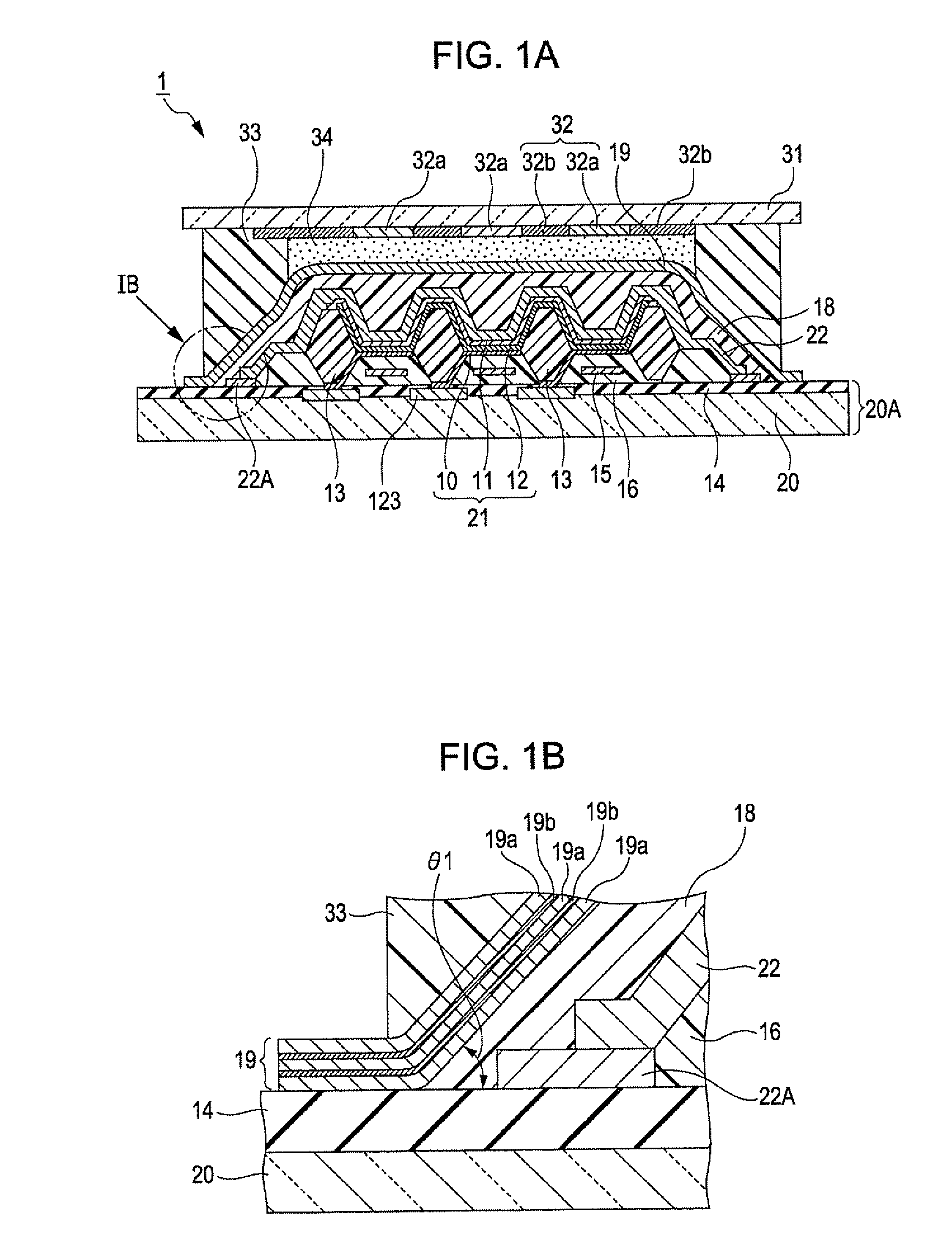
[0053]An organic electroluminescence device (organic EL device) according to a first Embodiment of the invention will now be described with reference to FIGS. 1A, 1B, 2A to 2C, 3, 4A, 4B, 5A to 5C, 6A, and 6B. Incidentally, in all the following drawings, film thickness of each component, ratios of sizes, and so on are appropriately changed for easy understanding of the drawings.

[0054]FIGS. 1A and 1B are cross-sectional views schematically showing an organic EL device 1. The organic EL device according to the invention is a so-called “top-emission-type” organic EL device. In the top emission system, light is drawn from an opposite substrate side, not from the side of a substrate on which organic EL elements are arranged. Therefore, the light emission area is not affected by the sizes of various types of circuits arranged on the element substrate, and a large light emission area can be effectively secured. Accordingly, high brightness can be secured, while suppressin...

second embodiment

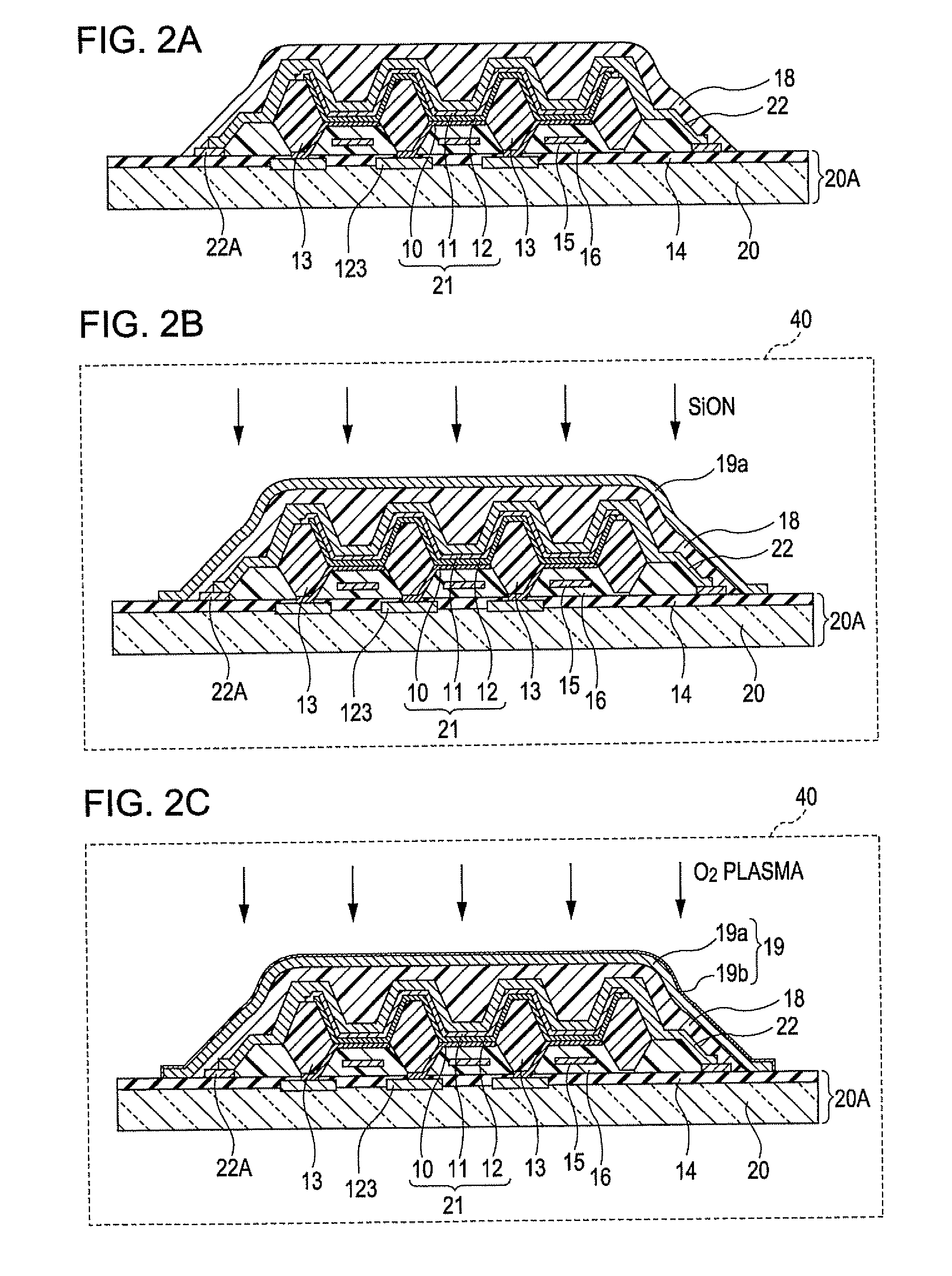
[0145]FIGS. 7A and 7B are explanatory diagrams of an organic EL device according to a second Embodiment of the invention. The organic EL device of this Embodiment is partially the same as the organic EL device of the first Embodiment. A difference between them is that the auxiliary wiring does not function as the protection layer of the cathode and an electrode-protecting layer for protecting the cathode is provided. Accordingly, in this Embodiment, the same components as those in the first Embodiment are denoted by the same reference numerals, and the detailed descriptions thereof are omitted.

[0146]As shown in FIG. 7A, auxiliary cathode wiring 24 for assisting electrical conduction between a cathode 11 and cathode wiring 22A is provided at the end of the cathode 11, and an electrode-protecting layer 17 covers the entire surfaces of the cathode 11, the cathode wiring 22A, and the auxiliary cathode wiring 24. This electrode-protecting layer 17 can prevent the cathode 11 and the under...

example

[0157]An Example of the invention will now be described. In this Example, a test device for evaluation was produced as an organic EL device in order to confirm effect of the invention.

[0158]The test device used in this Example was produced by forming a magnesium film (mg film) on a glass support substrate, forming a thin-film sealing layer consisting of an electrode-protecting layer (SiON) / an organic buffer layer / a gas barrier layer so as to cover the Mg film, and bonding a glass opposite substrate to the thin-film sealing layer. The electrode-protecting layer was in contact with the support substrate so as to seal the Mg film and was also in contact with the gas barrier layer so as to seal the organic buffer layer.

[0159]The thicknesses of components of the test device used were as follows: Mg film: 50 nm, electrode-protecting layer (SiON): 400 nm, organic buffer layer: 3 μm, and gas barrier layer: 400 nm. In the test device of this Example, the gas barrier layer was composed of sta...


PUM


Abstract

An organic electroluminescence device includes a substrate, a plurality of light-emitting elements arranged on the substrate, each including a pair of electrodes and an organic light-emitting layer disposed between the electrodes, an organic buffer layer covering the plurality of light-emitting elements, and a gas barrier layer covering the organic buffer layer. The gas barrier layer has a structure wherein first inorganic films and second inorganic films are alternately stacked. The first inorganic films contain a silicon compound containing nitrogen, the second inorganic films contain an oxide of the formation material of the first inorganic films and each have a thickness smaller than that of each first inorganic film. The numbers of the first inorganic films and the second inorganic films are each at least two.

Description

BACKGROUND[0001]1. Technical Field[0002]The present invention relates to an organic electroluminescence device, a process of producing an organic electroluminescence device, and an electronic apparatus.[0003]2. Related Art[0004]With diversification of information apparatuses, needs for flat displays that consume lower amounts of power and are reduced in weights have increased. As an example of such flat displays, organic electroluminescence devices (hereinafter, referred to as “organic EL devices”) having organic light-emitting layers are known.[0005]The organic EL device includes a plurality of organic light-emitting elements (organic EL elements) having a configuration wherein an organic light-emitting layer (light-emitting layer) or a functional layer such as an electron injection layer is disposed between an anode and a cathode. Among these components, the cathode and the electron injection layer are made of materials having properties of easily releasing electrons and thereby r...

Claims


Application Information

Patent Timeline
Patent Type & Authority Applications(United States)
IPC IPC(8): H01J1/62B05D5/06
CPCH01L51/5237H10K50/8426H10K50/8445H05B33/04H10K50/84H10K2102/103
Inventor HAYASHI, KENJI
Owner SEIKO EPSON CORP
Why Eureka
Try Eureka