Semiconductor integrated circuit device

Active Publication Date: 2010-01-28
RENESAS ELECTRONICS CORP
View PDF3 Cites 11 Cited by
  • Summary
  • Abstract
  • Description
  • Claims
  • Application Information

AI Technical Summary

Benefits of technology

[0022]The advantageous effects achieved by the preferred embodiments of the present invention are briefly summarized as follows:
[0023](1) A DC supply voltage can be supplied accurately with less voltage drop.
[0024](2) T

Problems solved by technology

However, the present inventors have found that the above technique for preventing the supply voltage supplied by the regulator from dropping has the following problem.
In recent years, there has been a tendency that nonvolatile memories have a larger memory capacity and thus require a larger current.
Multilayered

Method used


Image

  • Semiconductor integrated circuit device
  • Semiconductor integrated circuit device
  • Semiconductor integrated circuit device

Examples


Example

First Embodiment

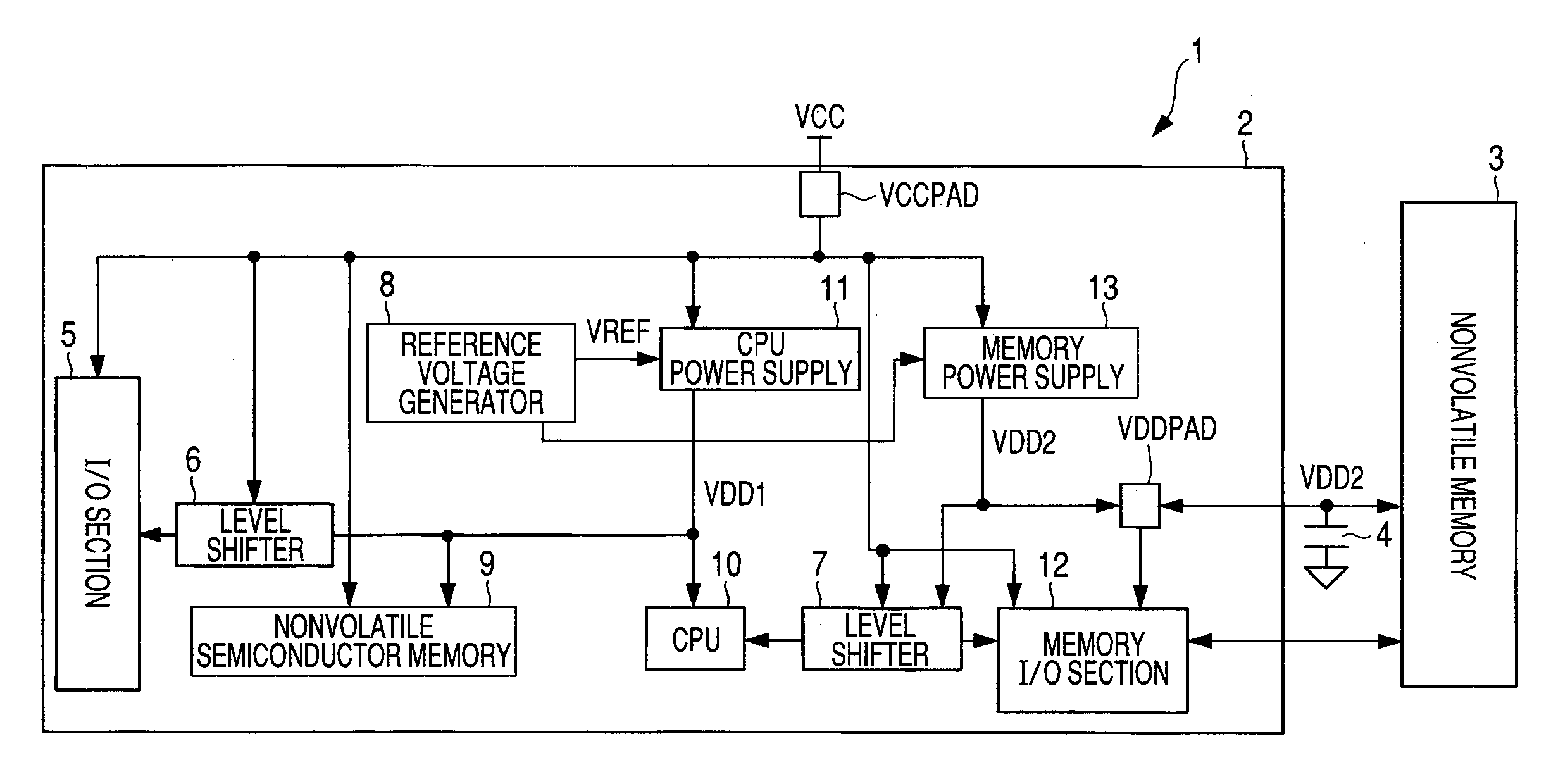
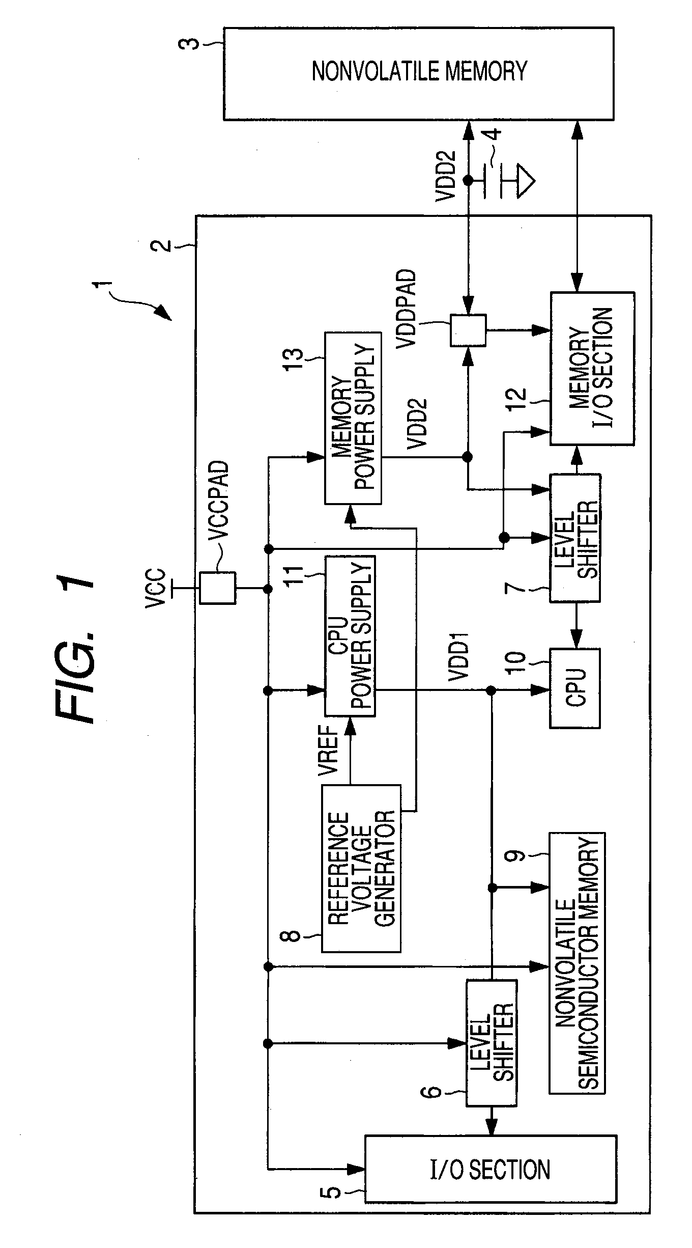
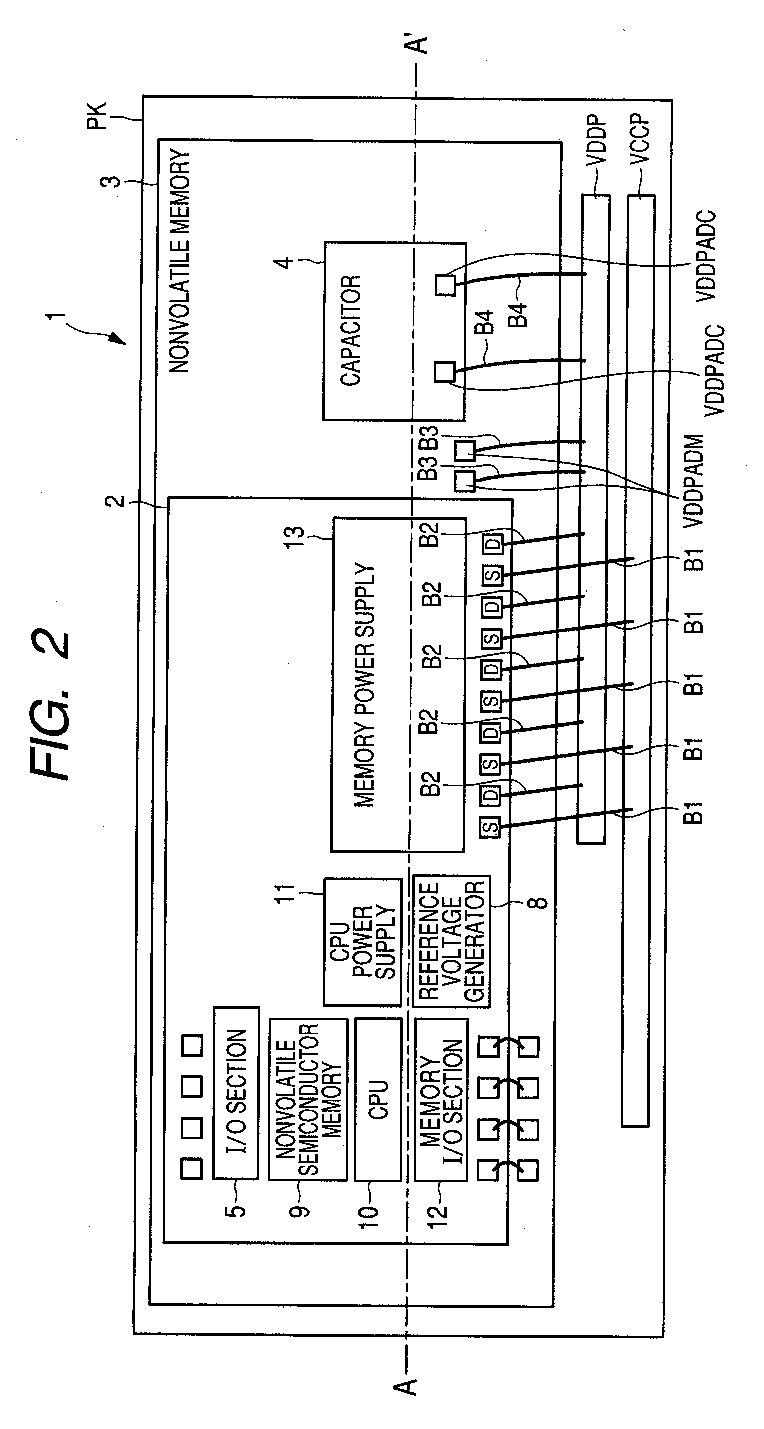
[0046]FIG. 1 is a block diagram showing the configuration of a semiconductor integrated circuit device according to a first embodiment of the present invention; FIG. 2 illustrates an example of package layout of the semiconductor integrated circuit device shown in FIG. 1; FIG. 3 is a sectional view taken along A-A′ in FIG. 2; FIG. 4 shows an example of the arrangement and connection pattern of source pads and drain pads in a memory power supply of the semiconductor integrated circuit device in FIG. 1; FIG. 5 illustrates an example of the layout pattern of the transistors in the memory power supply shown in FIG. 4; FIG. 6 is a sectional view taken along the line A-A′ in FIG. 5; FIG. 7 is a sectional view taken along the line B-B′ in FIG. 5; FIG. 8 illustrates an example of the arrangement of drain wirings and source wirings in the memory power supply in FIG. 4; and FIG. 9 illustrates the arrangement of drain wirings and source wirings in the memory power supply which ...

Example

Second Embodiment

[0091]FIG. 10 illustrates an example of package layout of a semiconductor integrated circuit device according to a second embodiment of the present invention and FIG. 11 is a sectional view taken along the line A-A′ in FIG. 10.

[0092]As in the foregoing first embodiment (FIG. 1), a semiconductor integrated circuit device 1 in the second embodiment includes a microcomputer 2, a nonvolatile memory 3, and a capacitor 4. The microcomputer 2 and the nonvolatile memory 3 are each formed on a single semiconductor chip.

[0093]The difference from the first embodiment is the package layout of the semiconductor integrated circuit device 1.

[0094]FIG. 10 illustrates an example of package layout of a semiconductor integrated circuit device according to the second embodiment of the present invention and FIG. 11 is a sectional view taken along the line A-A′ in FIG. 10.

[0095]As shown in FIG. 10, the nonvolatile memory 3 semiconductor chip lies in an upper part of a package substrate P...

Example

Third Embodiment

[0105]FIG. 12 illustrates an example of the arrangement and connection pattern of source pads S and drain pads D in the memory power supply according to a third embodiment of the present invention; FIG. 13 illustrates an example of the layout pattern of transistors T in the memory power supply shown in FIG. 12; FIG. 14 is a sectional view taken along the line A-A′ in FIG. 13; and FIG. 15 is a sectional view taken along the line B-B′ in FIG. 13.

[0106]In the third embodiment, the semiconductor integrated circuit device 1 includes a microcomputer 2, a nonvolatile memory 3 and a capacitor 4 as in the first embodiment (FIG. 1). The microcomputer 2 and the nonvolatile memory 3 are each formed on a single semiconductor chip.

[0107]In the third embodiment, pads of the same type are grouped together unlike the first embodiment in which the drain pads D and source pads S in the memory power supply 13 are alternately arranged.

[0108]FIG. 12 illustrates an example of the arrangeme...


PUM


Abstract

A semiconductor integrated circuit device which substantially reduces drop in a supply voltage generated by a regulator and ensures stable supply of a supply voltage with high efficiency and high accuracy. In the device, a memory power supply includes a plurality of transistors and an error amplifier. In the transistors, source pads and drain pads are alternately arranged in a row along one edge of a semiconductor chip in a peripheral area of the chip. Transistor gates are formed in parallel with the alternately arranged source pads and drain pads (so that the longitudinal direction of the gates is parallel to the direction of the arrangement of the source pads and drain pads). Consequently, the length of wirings coupled to drains and sources is shortened and the sheet resistance is decreased.

Description

CROSS-REFERENCE TO RELATED APPLICATIONS [0001]The disclosure of Japanese Patent Application No. 2008-188144 filed on Jul. 22, 2008 including the specification, drawings and abstract is incorporated herein by reference in its entirety.BACKGROUND OF THE INVENTION[0002]The present invention relates to technology for power supply generation by a regulator and more particularly relates to technology for supplying a supply voltage in system-in-packages.[0003]In the semiconductor integrated circuit device field, a system-in-package (SiP) is known in which more than one semiconductor chip are mounted in a single package.[0004]System-in-package type semiconductor integrated circuit devices include those in which a system LSI such as a microcomputer and a large-capacity nonvolatile memory are packaged and it is known that some of such semiconductor integrated circuit devices incorporate an on-chip regulator to drive the nonvolatile memory.[0005]In recent years, as the tendency for electronic ...

Claims


Application Information

Patent Timeline
IPC IPC(8): G05F3/08
CPCG11C16/30H01L23/4824H01L27/0207H01L27/0218H01L27/11526H01L2924/0002H01L27/11573H01L2924/00H01L2224/48091H01L2224/48227H01L2924/19107H10B41/40H10B43/40H01L2924/00014
Inventor ARISAKA, NAOYAITO, TAKAYASU
Owner RENESAS ELECTRONICS CORP
Why Eureka
Try Eureka