Semiconductor integrated circuit having latch circuit applied changeable capacitance and method thereof

a latch circuit and integrated circuit technology, applied in the field of semiconductor integrated circuits, can solve the problems of insignificant variation in voltage at storage nodes, electric noise generation, soft error is a temporary malfunction, etc., and achieve the effect of reducing the amount of charge transfer and increasing electrical capacity

Inactive Publication Date: 2010-01-28
RENESAS ELECTRONICS CORP
View PDF3 Cites 37 Cited by
  • Summary
  • Abstract
  • Description
  • Claims
  • Application Information

AI Technical Summary

Benefits of technology

[0016]According to the exemplary aspect of the present invention, at the time of latching, the capacitive element is connected to the first and second inverter circuits to increase the electrical capacity. The logical level of latched data is thereby made not easily invertible. On the other hand, at the time of pass-through, the voltages at the first end and the second end are averaged by the malfunction-preventing selector circuit group, thereby enabling reducing the amount of charge transfer between the output end of the first inverter circuit and the first terminal when a change from the pass-through state to the latching state is again made. The same effect as that between the output end of the first inverter circuit and the first end is achieved between the output end of the second inverter circuit and the second end. As a result, changes in voltage at the output ends of the first inverter circuit and the second inverter circuit can be reduced to prevent a malfunction.

Problems solved by technology

In some case, electrical noise is generated in a semiconductor circuit by a radioactive ray to cause a malfunction.
In general, a soft error is a temporary malfunction.
For example, in the case of a latch circuit included in a semiconductor integrated circuit, a variation in voltage at a storage node is insignificantly small if the charge capacity of the storage node is sufficiently large.
That is, in recent years, a malfunction due to a radioactive ray in a latch circuit included in a semiconductor integrated circuit can become a fixed error.
That is, incorrect data may be latched.
Thus, a long period is required to sufficiently invert the potential enough to correctly latch the data by the latch circuit.
Accordingly, this technology has a problem in point of view of the high speed operation.
The logical level of latched data is thereby made not easily invertible.

Method used


Image

  • Semiconductor integrated circuit having latch circuit applied changeable capacitance and method thereof
  • Semiconductor integrated circuit having latch circuit applied changeable capacitance and method thereof
  • Semiconductor integrated circuit having latch circuit applied changeable capacitance and method thereof

Examples


first exemplary embodiment

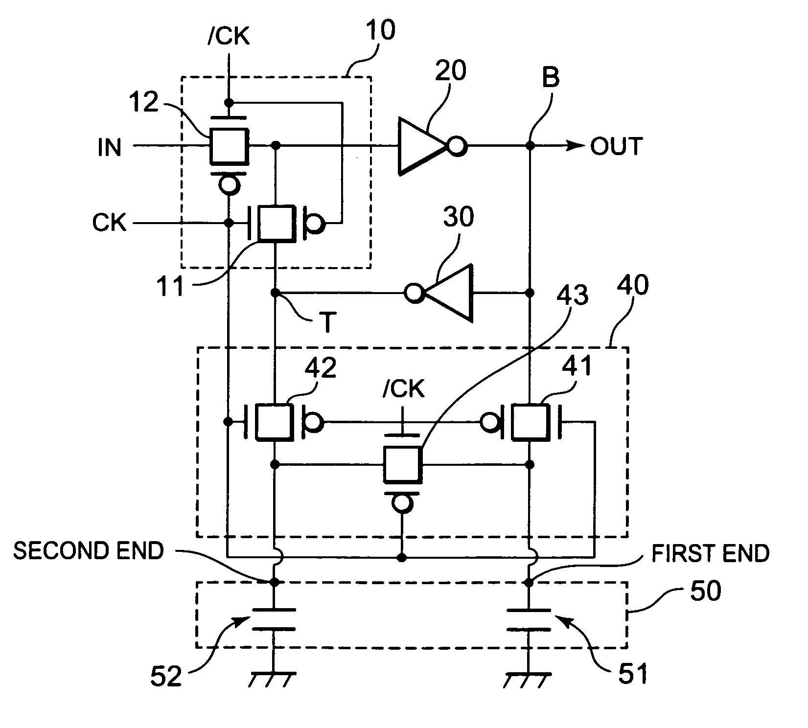
[0027]FIG. 2 is a circuit diagram showing a semiconductor integrated circuit according to a first exemplary embodiment. This semiconductor integrated circuit is provided with an input end IN and an output end OUT. This semiconductor integrated circuit receives an input signal from the input end IN and outputs an output signal to the output end OUT.

[0028]The semiconductor integrated circuit has a flip-flop circuit, a capacitive element and a switch circuit, as shown in outline. The switch circuit includes a first switch circuit and a second switch circuit. The first switch circuit couples the capacitive element to two nodes of the flip-flop circuit at a predetermined timing. The second switch circuit short-circuits ends of the capacitive element connected to the two nodes at a timing different from the predetermined timing.

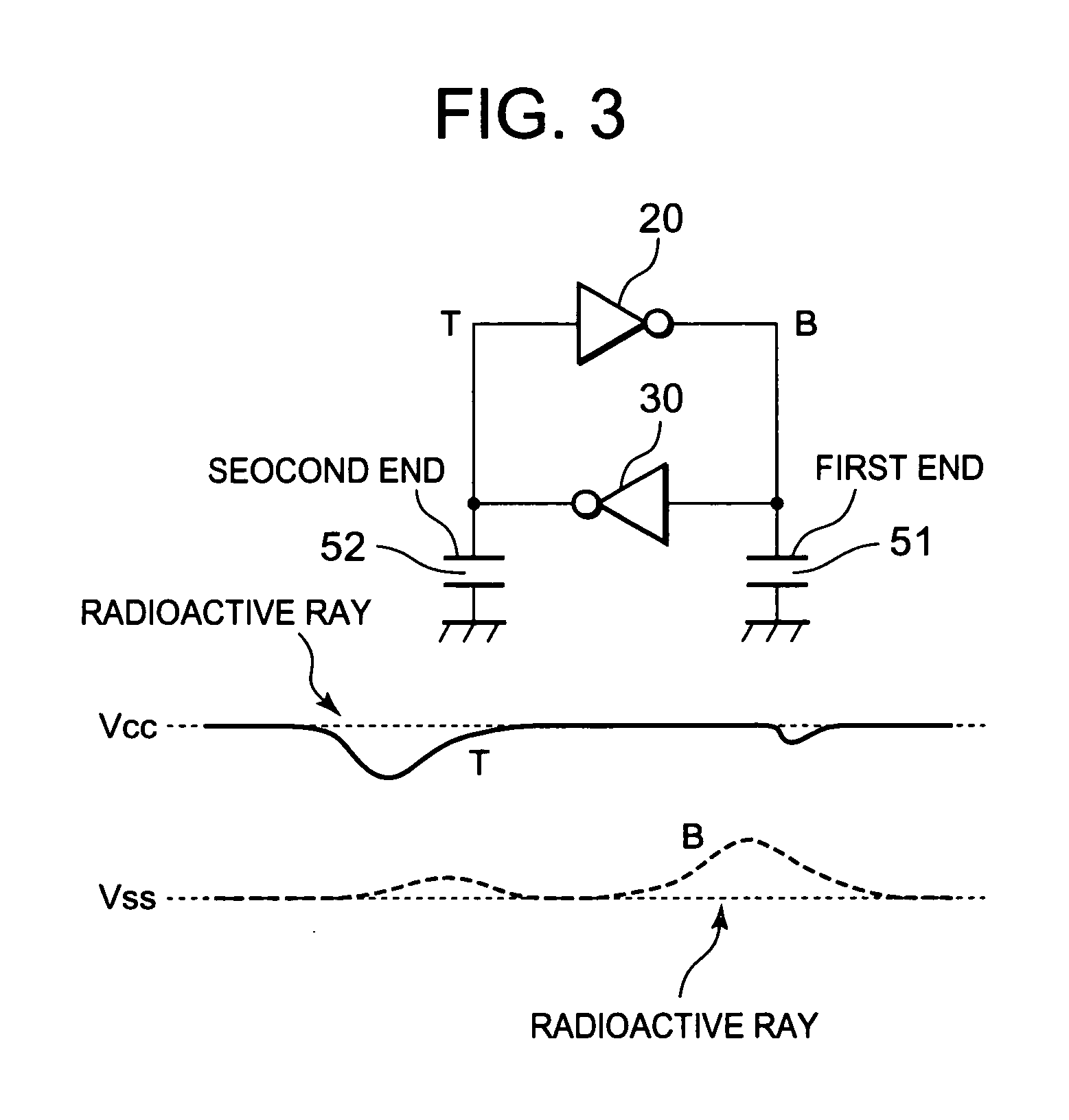
[0029]More specifically, as shown in FIG. 2, the semiconductor integrated circuit has, as the above-mentioned flip-flop circuit, a first inverter circuit 20, a sec...

second exemplary embodiment

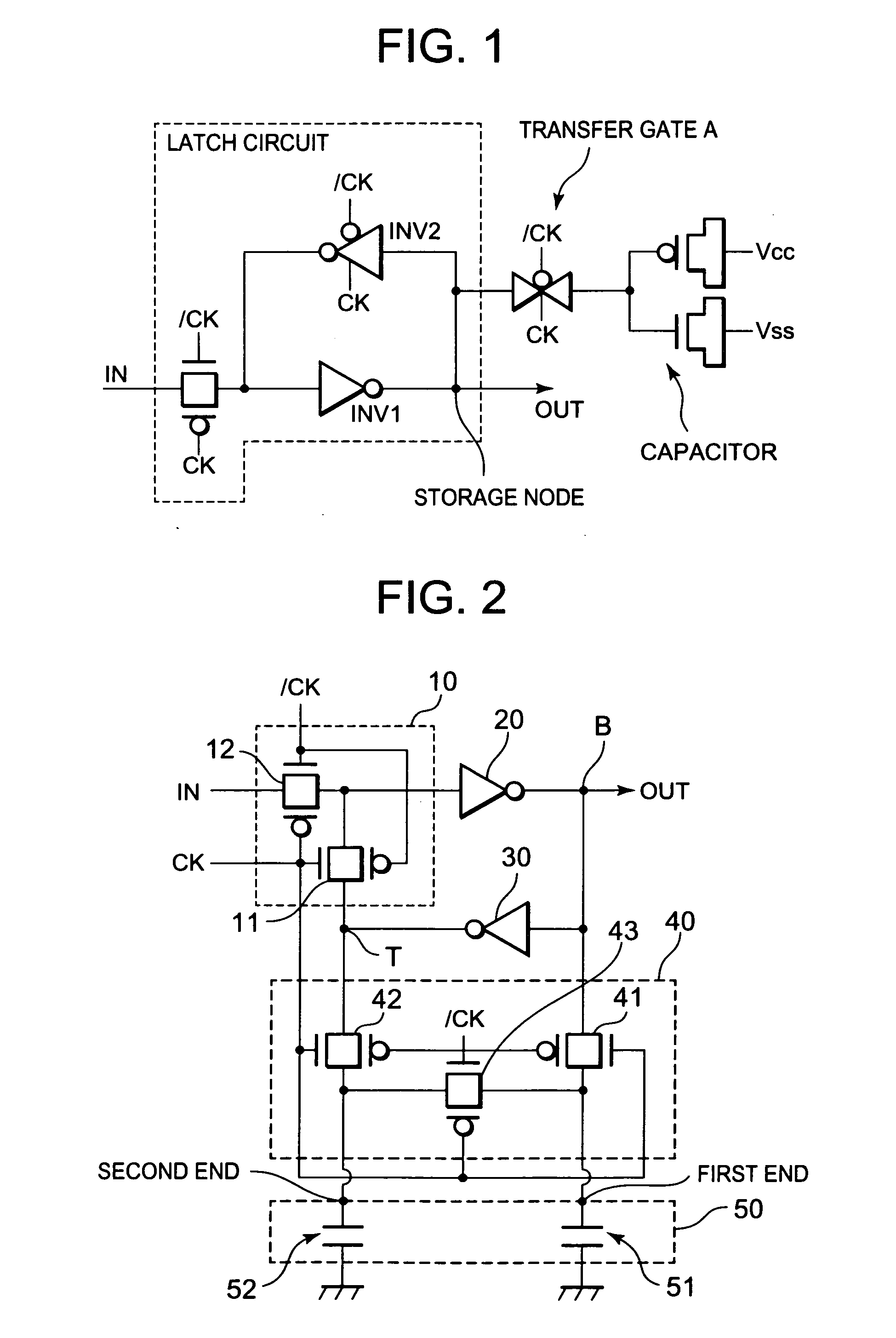
[0052]A second exemplary embodiment of the present invention will next be described. In the second exemplary embodiment, the configuration in the capacitive element group 50 is changed from that in the first exemplary embodiment. In the first exemplary embodiment, two capacitors (first capacitor 51 and second capacitor 53) are used as the capacitive element group 50. In the second exemplary embodiment, one capacitor is used as the capacitive element group 50. In other respects, the second exemplary embodiment is the same as the first exemplary embodiment. Therefore the detailed description for the present exemplary embodiment will not be repeated.

[0053]FIG. 5 is a circuit diagram showing a semiconductor integrated circuit according to the second exemplary embodiment. In the second exemplary embodiment, a capacitor 53 is provided as the capacitive element group 50. One end (the first end) of the capacitor 53 is connected to the storage node B through the transfer gate 41 in the malfu...


PUM


Abstract

A semiconductor integrated circuit includes a flip-flop circuit, a capacitive element, and a switch circuit. The switch circuit includes a first switch circuit which couples the capacitive element to two nodes of the flip-flop circuit at a first timing, and a second switch circuit which short-circuits ends of the capacitive element connected to the two nodes at a second timing different from the first timing.

Description

INCORPORATION BY REFERENCE[0001]This application is based upon and claims the benefit of priority from Japanese Patent Application No. 2008-192796 which was filed on Jul. 25, 2008, the disclosure of which is incorporated herein in its entirety by reference.BACKGROUND OF THE INVENTION[0002]1. Field of the Invention[0003]The present invention relates to a semiconductor integrated circuit and, more particularly, to a semiconductor integrated circuit having a latch circuit and a method of preventing a semiconductor integrated circuit from malfunctioning.[0004]2. Description of Related Art[0005]In some case, radioactive rays penetrate a semiconductor integrated circuit. Alpha rays, neutron rays and the like are conceivable as such radioactive rays. In some case, alpha rays are generated when a radioactive isotope contained in a semiconductor integrated circuit package or wiring. Neutron rays derive from cosmic rays. In some case, electrical noise is generated in a semiconductor circuit b...

Claims


Application Information

Patent Timeline
Patent Type & Authority Applications(United States)
IPC IPC(8): H03K17/00
CPCG11C5/005G11C11/4125H03K19/00338H03K3/0375H03K3/356121H03K3/013
Inventor MONDEN, JUNJI
Owner RENESAS ELECTRONICS CORP
Why Eureka
Try Eureka