Method for improving surface roughness of processed film of substrate and apparatus for processing substrate

a technology of surface roughness and processing film, which is applied in the direction of instruments, basic electric elements, printing, etc., can solve the problems of failure to manufacture a semiconductor device of a desired quality, and achieve the effect of improving yield and surface roughness of treatment film on the substra

Inactive Publication Date: 2010-01-28
TOKYO ELECTRON LTD
View PDF14 Cites 130 Cited by
  • Summary
  • Abstract
  • Description
  • Claims
  • Application Information

AI Technical Summary

Benefits of technology

[0025]According to the present invention, the surface roughness of the treatment film on the substrate can be improved so that, for example, a circuit pattern having a predetermined dimension is formed on a substrate, and, for example, subsequent etching treatment or the like is preferably performed, resulting in improved yields.

Problems solved by technology

As a result of the appearance of projections and depressions on the surface of the base film due to the formation of the vertical lines in the base film, a precise circuit pattern is no longer formed on the wafer, thus resulting in a failure to manufacture a semiconductor device with a desired quality.
Particularly, in these days when the circuit pattern has been made finer, even slight projections and depressions greatly affect the shape of the circuit pattern, and therefore it is an important problem to improve the surface roughness of the resist film.

Method used


Image

  • Method for improving surface roughness of processed film of substrate and apparatus for processing substrate
  • Method for improving surface roughness of processed film of substrate and apparatus for processing substrate
  • Method for improving surface roughness of processed film of substrate and apparatus for processing substrate

Examples


Embodiment Construction

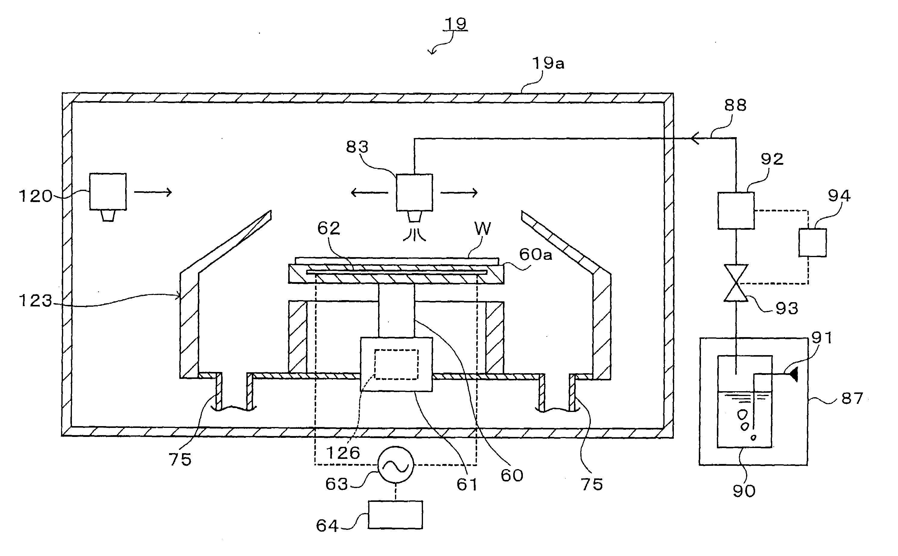
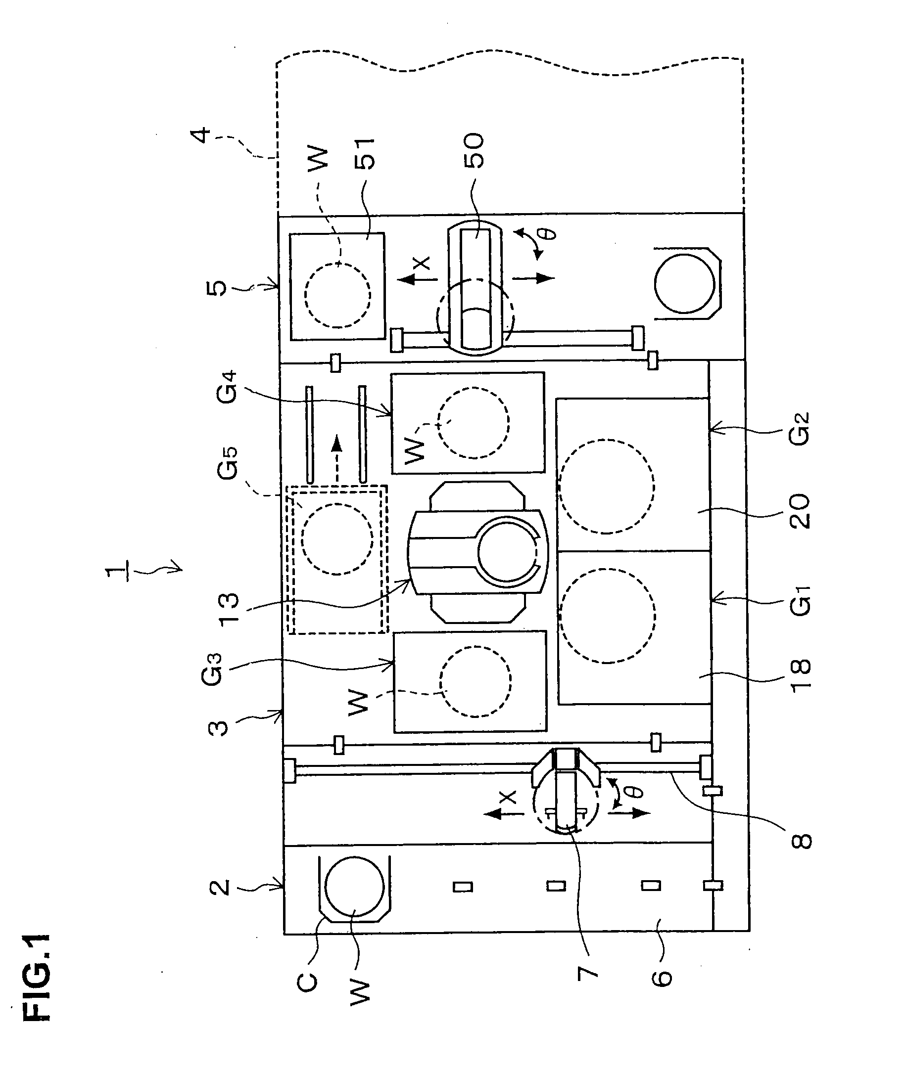
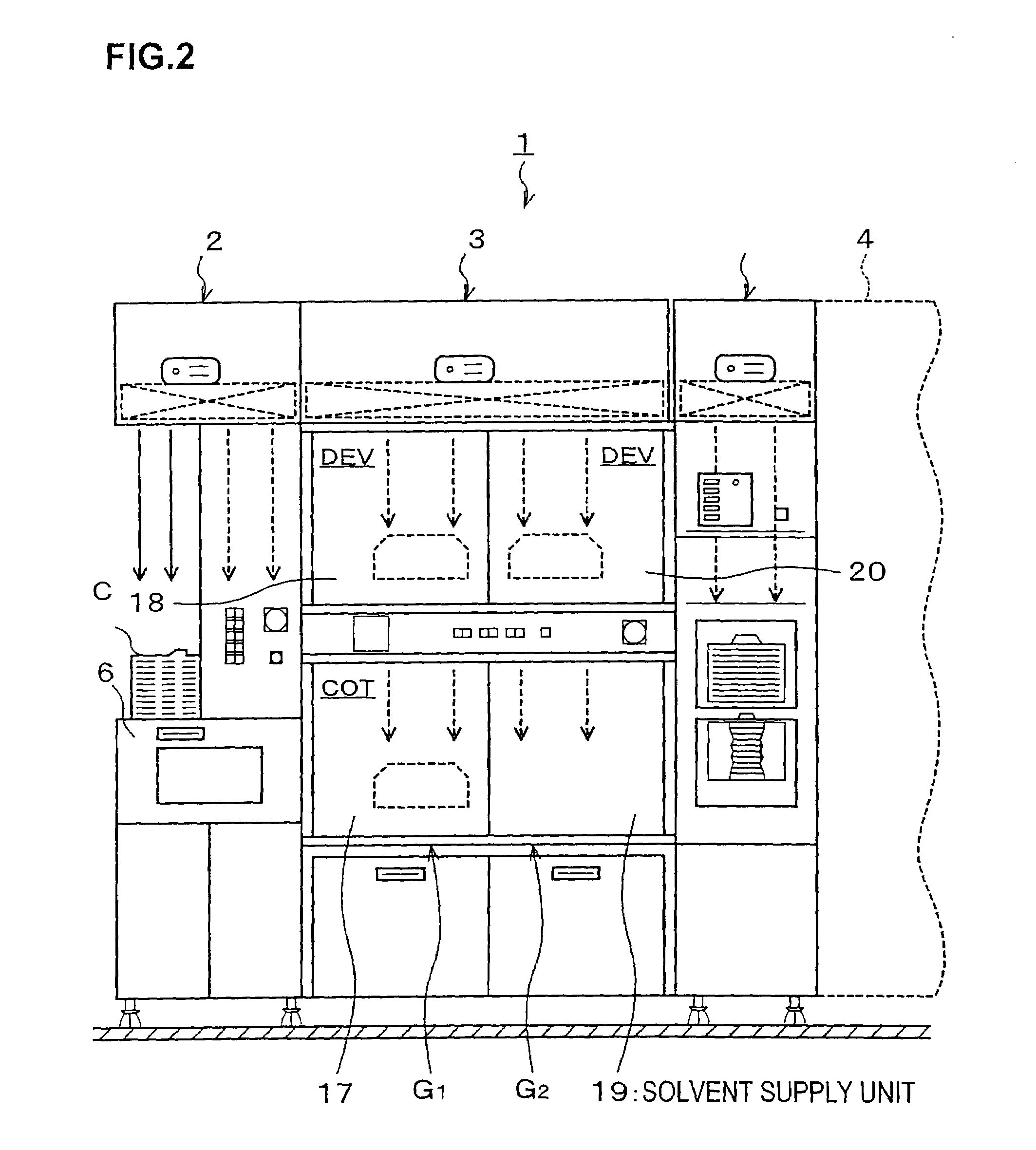
[0066]Hereinafter, a preferred embodiment of the present invention will be described. FIG. 1 is a plan view showing the outline of a configuration of a coating and developing treatment system 1 incorporating a substrate treatment apparatus according to the present embodiment, FIG. 2 is a front view of the coating and developing treatment system 1, and FIG. 3 is a rear view of the coating and developing treatment system 1.

[0067]The coating and developing treatment system 1 has, as shown in FIG. 1, a configuration in which, for example, a cassette station 2 for carrying, for example, 25 wafers per cassette as a unit from / to the outside into / from the coating and developing treatment system 1 and carrying the wafers W into / out of the cassette C; a processing station 3 including various kinds of processing and treatment units, which are multi-tiered, for performing predetermined processing or treatments in a manner of single wafer processing in coating and developing treatment processes;...


PUM

PropertyMeasurementUnit
wavelengthaaaaaaaaaa
temperatureaaaaaaaaaa

Abstract

A treatment apparatus for treating a substrate on a surface of which a treatment film has been formed and subjected to exposure processing and developing treatment. The treatment apparatus includes a nozzle for supplying a solvent gas of the treatment film to the surface of the treatment film on the substrate, and a moving mechanism for moving the nozzle which is supplying the solvent gas, relative to the substrate. The nozzle has an elongated discharge portion at least longer than a diameter of the substrate and partition plates at a front and a rear in the moving direction of the nozzle.

Description

CROSS-REFERENCE TO RELATED APPLICATIONS[0001]This application is a division of U.S. application Ser. No. 10 / 559,332, filed May 30, 2006, which is the National Stage of PCT / JP2004 / 007486, filed May 31, 2004, and claims the benefit of priority of Japanese application 2003-162054, filed Jun. 6, 2003. The entire contents of U.S. application Ser. No. 10 / 559,332, are incorporated herein by reference.TECHNICAL FIELD[0002]The present invention relates to a method of improving surface roughness of a treatment film on a substrate and a substrate treatment apparatus.BACKGROUND ART[0003]In a photolithography process in a manufacturing process of a semiconductor device, for example, resist coating treatment in which a resist solution is applied onto a base film of a semiconductor wafer (hereinafter, referred to as a “wafer”) to form a resist film; exposure processing in which a predetermined pattern is exposed on the wafer; developing treatment in which the wafer after exposure is developed; etc...

Claims


Application Information

Patent Timeline
Patent Type & Authority Applications(United States)
IPC IPC(8): G03B27/52G03F7/40H01L21/00H01L21/027
CPCG03F7/40H01L21/0273H01L21/67178H01L21/6715H01L21/67109
Inventor INATOMI, YUICHIRO
Owner TOKYO ELECTRON LTD
Why Eureka
Try Eureka