Photovoltaic device and method of manufacturing the same

a photovoltaic device and photoelectric conversion technology, applied in the field of photovoltaic devices, can solve the problems of difficult to obtain the improvement of photoelectric conversion efficiency, increase in manufacturing costs of photovoltaic devices, etc., and achieve the effect of improving the photoelectric conversion efficiency of photovoltaic devices

Inactive Publication Date: 2010-02-04
SAMSUNG DISPLAY CO LTD +1
View PDF6 Cites 54 Cited by
  • Summary
  • Abstract
  • Description
  • Claims
  • Application Information

AI Technical Summary

Benefits of technology

[0012]According to the above, the plurality of first protrusions are formed on the light incidence surface of the semiconductor substrate, and the plurality of second protrusions are additionally formed on the plurality of surfaces of the plurality of first protrusions. Accordingly, light, which is introduced into the semiconductor substrate from an exterior through the light incidence surface, may be scattered by the plurality of first and second protrusions formed on the light incidence surface. Accordingly, an optical path of the light may be lengthened in the semiconductor substrate, so that photoelectric conversion efficiency of the photovoltaic device can be improved.

Problems solved by technology

Although the photoelectric conversion efficiency of the photovoltaic device may increase by enlarging the thickness of the semiconductor layer to lengthen a path of light traveling in the semiconductor layer, the manufacturing costs and manufacturing time of the photovoltaic device may increase if the thickness of the semiconductor layer increases.
In addition, as the characteristic of the fill factor may degraded, improvement in the photoelectric conversion efficiency may be difficult to obtain.

Method used


Image

  • Photovoltaic device and method of manufacturing the same
  • Photovoltaic device and method of manufacturing the same
  • Photovoltaic device and method of manufacturing the same

Examples


Embodiment Construction

[0023]Hereinafter, exemplary embodiments of the present invention will be described in detail with reference to accompanying drawings. It is understood that the present invention should not be limited to the following exemplary embodiments but various changes and modifications can be made by one ordinary skilled in the art within the spirit and scope of the present invention. The present invention is defined only by the scope of the appended claims. Meanwhile, elements shown in the drawings can be simplified or magnified for the purpose of clear explanation. In addition, the same reference numerals are used to designate the same elements throughout the drawings.

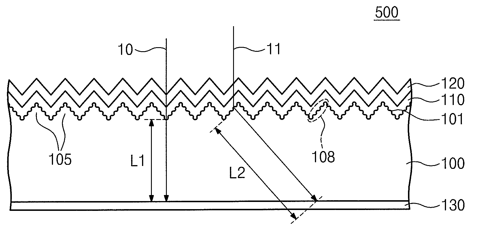
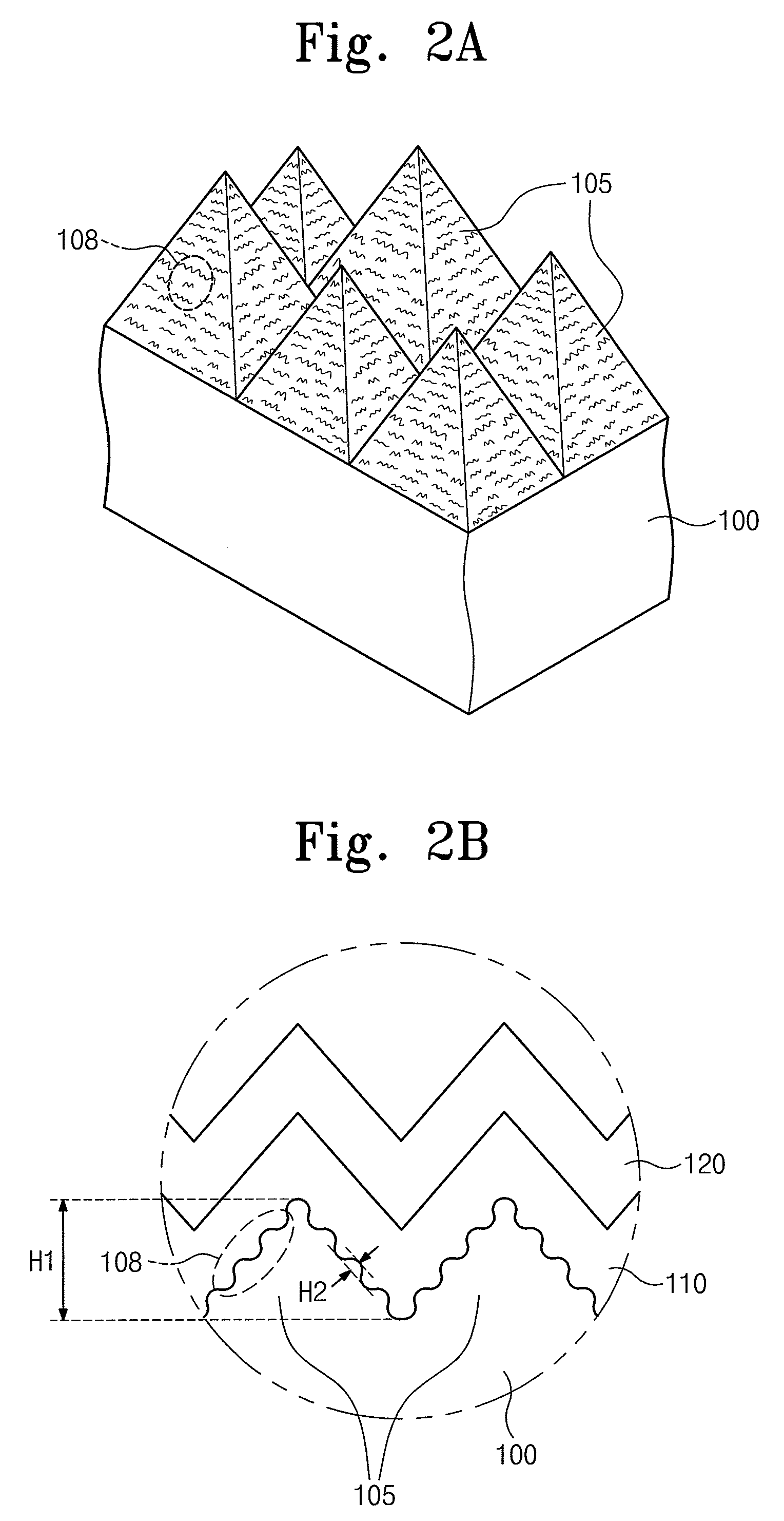
[0024]FIG. 1 is a sectional view showing an exemplary embodiment of a photovoltaic device according to the present invention.

[0025]Referring to FIG. 1, a photovoltaic device 500 includes a semiconductor substrate 100, a semiconductor layer 110, a first electrode 120, and a second electrode 130.

[0026]The semiconductor substrat...


PUM


Abstract

A method of manufacturing a photovoltaic device includes preparing a semiconductor substrate having a light incidence surface receiving light and including single crystalline silicon, wet-etching the light incidence surface to form a plurality of first protrusions on the light incidence surface, dry etching a plurality of surfaces of the first protrusions to form a plurality of second protrusions on the plurality of surfaces of the first protrusions, and forming a semiconductor layer on the light incidence surface. The method further includes forming a first electrode on the semiconductor layer and forming a second electrode on a rear surface of the semiconductor substrate facing the light incidence surface.

Description

CROSS-REFERENCE TO RELATED APPLICATION[0001]This application relies for priority upon Korean Patent Application No. 2008-75261 filed on Jul. 31, 2008, the contents of which are hereby incorporated by reference herein in their entirety.BACKGROUND[0002]1. Technical Field[0003]The present disclosure relates to a photovoltaic device and to a method of manufacturing the same. More particularly, the present disclosure relates to a photovoltaic device capable of improving photoelectric conversion efficiency and to a method of manufacturing the photovoltaic device.[0004]2. Description of the Related Art[0005]A photovoltaic device may convert optical energy into electric energy. Generally, the photovoltaic device includes a semiconductor layer which may induce photovoltaic effect by absorbing external optical energy, and first and second electrodes between which the semiconductor layer is interposed.[0006]Meanwhile, photoelectric conversion efficiency of the photovoltaic device may be determ...

Claims


Application Information

Patent Timeline
Patent Type & Authority Applications(United States)
IPC IPC(8): H01L31/00H01L21/302
CPCH01L31/02363Y02E10/50H01L31/035281H01L31/04H01L31/18H01L31/0236
Inventor OH, MIN-SEOKPARK, MINLEE, CZANG-HOSHIN, MYUNG-HUNLEE, BYOUNG-KYUNAM, YUK-HYUNJUNG, SEUNG-JAELIM, MI-HWASEO, JOON-YOUNG
Owner SAMSUNG DISPLAY CO LTD
Why Eureka
Try Eureka