Wiring substrate and electronic component device

a technology of electronic components and wiring substrates, applied in the field of wiring substrates and electronic components, can solve the problems of small rigidity and the readiness of warps, and achieve the effect of improving reliability and occurrence of warps

Inactive Publication Date: 2010-02-04
SHINKO ELECTRIC IND CO LTD
View PDF3 Cites 69 Cited by
  • Summary
  • Abstract
  • Description
  • Claims
  • Application Information

AI Technical Summary

Benefits of technology

[0015]As explained above, in the present invention, even when the thin wiring substrate without t

Problems solved by technology

In the above coreless wiring substrate in the prior art, such a problem exists that

Method used


Image

  • Wiring substrate and electronic component device
  • Wiring substrate and electronic component device
  • Wiring substrate and electronic component device

Examples


Embodiment Construction

[0025]An embodiment of the present invention will be explained with reference to the accompanying drawings hereinafter.

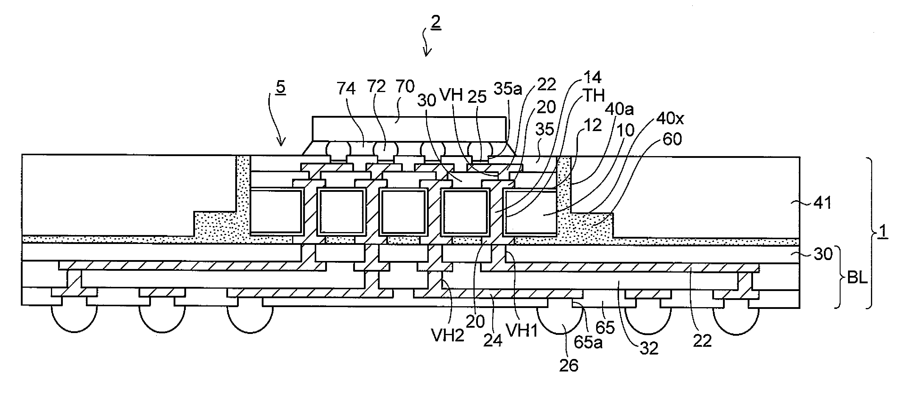
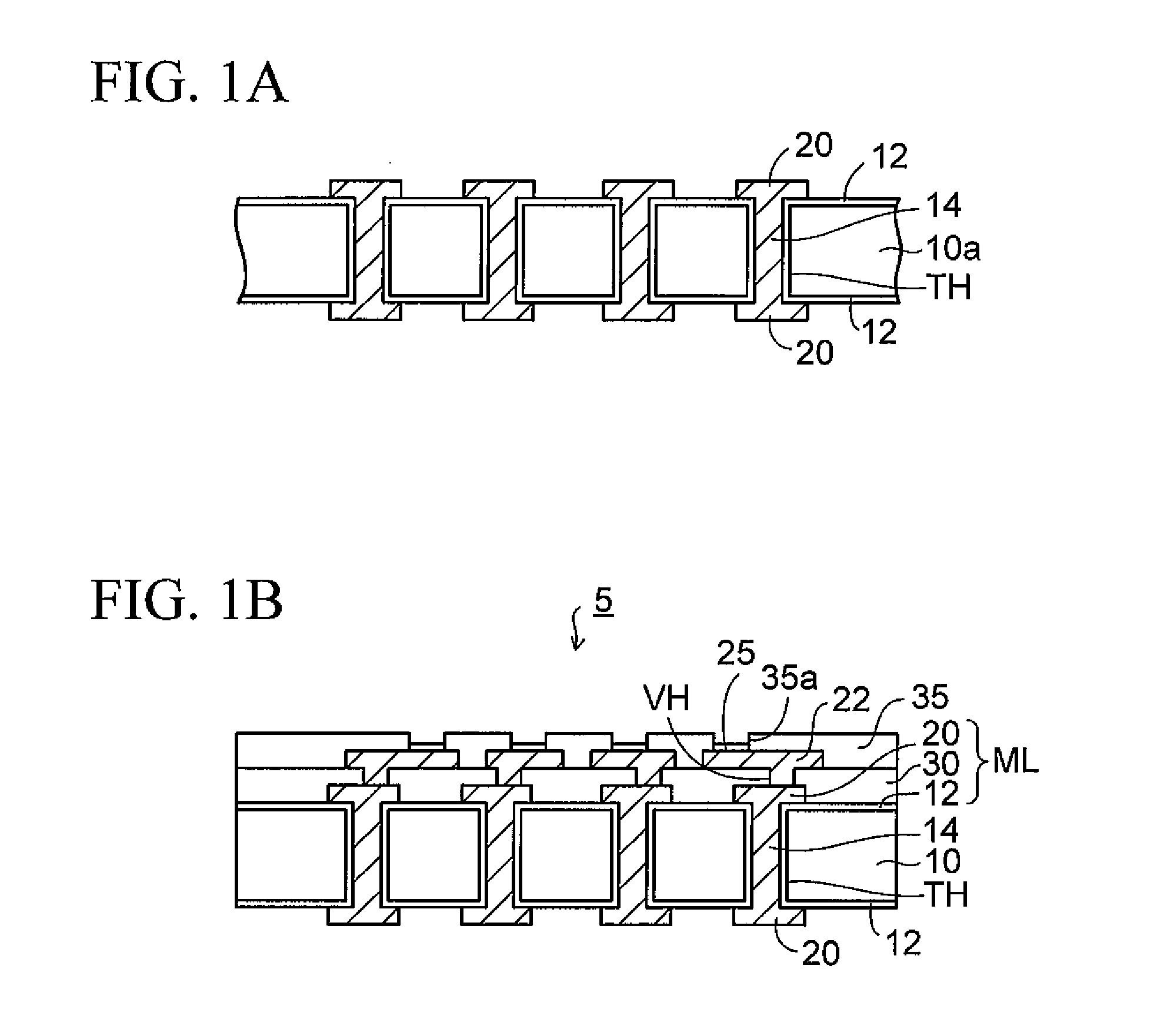
[0026]FIGS. 1A and 1B are sectional views showing a method of manufacturing an interposer built in a wiring substrate according to an embodiment of the present invention. At first, a method until a sectional structure shown in FIG. 1A is obtained will be explained hereunder. First, a thickness of a silicon wafer 10a is reduced to about 200 μm by grinding the silicon wafer 10a by using the grinder.

[0027]Then, a mask (not shown) in which opening portions are provided is formed on the silicon wafer 10a. Then, through holes TH are formed by penetration-processing the silicon wafer 10a to the thickness direction by means of the anisotropic dry etching (RIE, or the like) through the opening portions in the mask. Then, the mask is removed. The fine through holes TH whose diameter is 20 to 30 μm can be easily formed by using the anisotropic dry etching.

[0028]Then, a silicon...


PUM


Abstract

A wiring substrate includes a frame-shaped reinforcing plate in which an opening portion is provided in a center portion, an interposer arranged in the opening portion of the reinforcing plate and having such a structure that a wiring layer connected mutually via a through electrode is formed on both surface sides of a substrate respectively, a resin portion filled between a side surface of the interposer and a side surface of the opening portion of the reinforcing plate, and coupling the interposer and the reinforcing plate, and an n-layered (n is an integer of 1 or more) lower wiring layer connected the wiring layer on the lower surface side of the interposer to extend from the interposer to an outer area.

Description

CROSS-REFERENCE TO RELATED APPLICATIONS[0001]This application is based on and claims priority of Japanese Patent Application No. 2008-196449 filed on Jul. 30, 2008, the entire contents of which are incorporated herein by reference.BACKGROUND OF THE INVENTION[0002]1. Field of the Invention[0003]The present invention relates to a wiring substrate and an electronic component device and, more particularly, a wiring substrate on which an electronic component such as a semiconductor chip, or the like is mounted and an electronic component device constructed by mounting an electronic component on the wiring substrate.[0004]2. Description of the Related Art[0005]In the prior art, there is a wiring substrate on which an electronic component such as a semiconductor chip, or the like is mounted (electronic component mounting package). As such wiring substrate, there is a coreless wiring substrate from which a core substrate as a supporting base material is omitted in order to attain the thin t...

Claims


Application Information

Patent Timeline
IPC IPC(8): H05K1/16H05K1/11H05K1/09
CPCH01L2924/01078H01L2924/01079H01L2924/15311H01L2224/16H01L23/49816H01L23/49822H01L23/49833H01L21/4857H01L2924/00014H01L2924/00011H01L2224/16227H01L2924/3511H01L2224/73204H01L2224/32225H01L2224/04105H01L2224/0401H01L2224/16225H01L2924/00
Inventor ARAI, TADASHIKOBAYASHI, TOSHIO
Owner SHINKO ELECTRIC IND CO LTD
Why Eureka
Try Eureka