
Light Emitting Diode and Method for Manufacturing the Same

a technology of light-emitting diodes and manufacturing methods, which is applied in the direction of solid-state devices, nanotechnology, electric devices, etc., can solve the problems of complicated and expensive manufacturing steps of modifying the light-emitting diodes to obtain white light, and achieve the effects of reducing dimensionality on both sides, maximizing transmittance, and enhancing recombination ra

Inactive Publication Date: 2010-02-04
ECO SPARK
View PDF3 Cites 37 Cited by
  • Summary
  • Abstract
  • Description
  • Claims
  • Application Information

AI Technical Summary

Benefits of technology

"The present invention provides a light emitting diode with improved broadband spectral distribution and high brightness. The diode includes a p-doped structure and a plurality of n-doped ZnO nanowires arranged on the p-doped structure, with an insulating structure between the nanowires to electrically separate them. The insulating structure acts as an insulator between the nanowires and the substrate, while the transparent conductive layer acts as an electrical contact with the nanowires. The diode emits light with a wavelength of 200 nm to 700 nm. The insulating structure can be made of spin-on-glass, polymethylmethacrylate, SiO2, or epoxy resin. The diode can also have a conductor in electrical contact with the p-doped structure. The nanowire homo p-n junctions formed by the p-doped and n-doped ZnO nanowires have advantages over hetero junctions and nanowire / substrate homo p-n junctions. The tips of the nanowires are electrically connected to the transparent conductive layer for maximizing transmittance and minimizing resistance. The method for manufacturing the light emitting diode includes arranging the p-doped structure on the substrate, forming the n-doped ZnO nanowires, arranging the insulating structure among the nanowires, and arranging the transparent conductive layer on the insulating structure."

Problems solved by technology

However, due to disadvantages associated with thin-film technologies, present semiconductor technology seeks to utilize the advantages of nanowires in the areas of LEDs and laser diodes (LDs), where the nanowires are used as active components.
However, both the described methods for modifying the light emitting diode to obtain white light involve complicated and expensive manufacturing steps.

Method used


Image

  • Light Emitting Diode and Method for Manufacturing the Same
  • Light Emitting Diode and Method for Manufacturing the Same
  • Light Emitting Diode and Method for Manufacturing the Same

Examples


Embodiment Construction

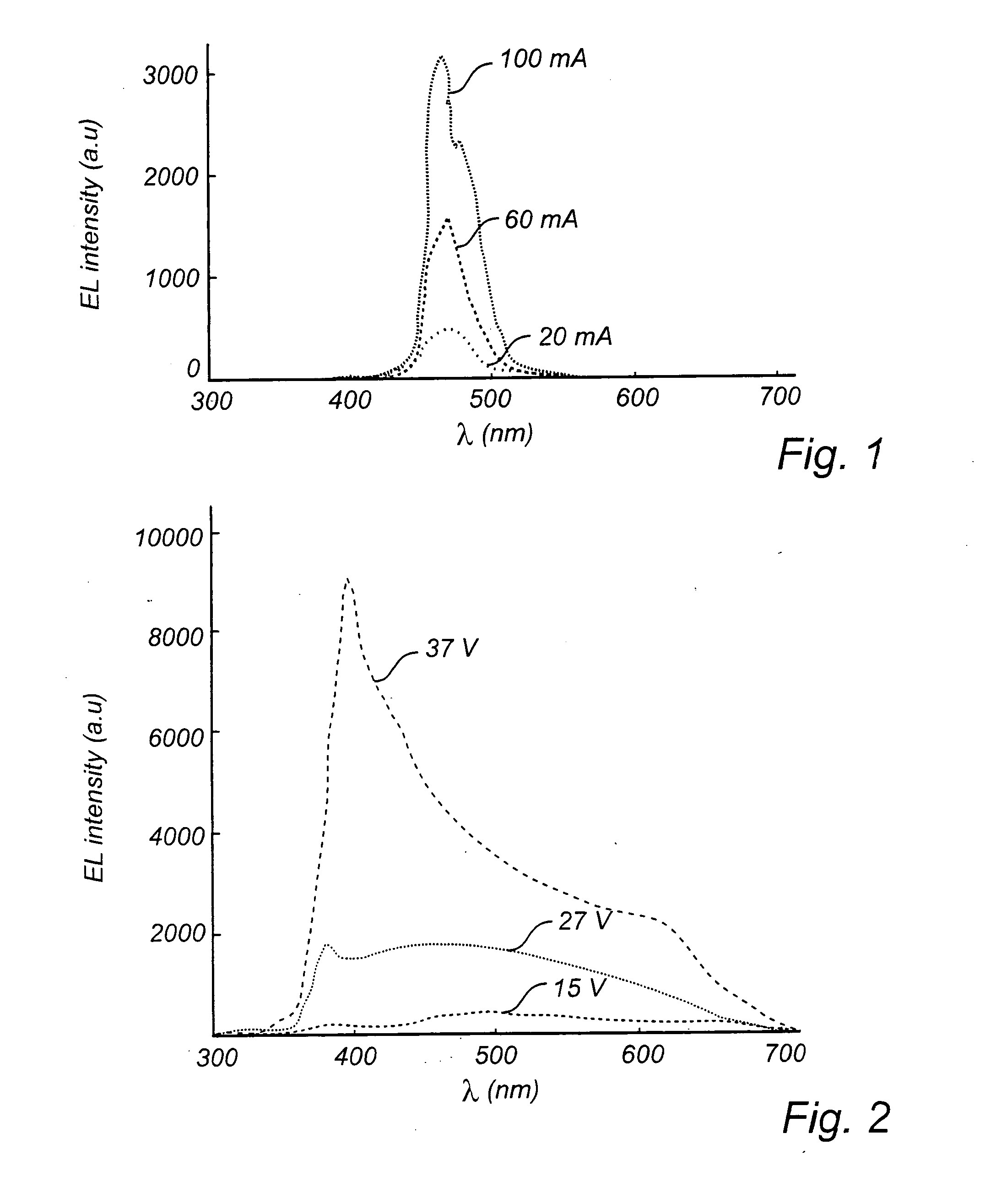
[0028]FIG. 2 is a graph showing the EL (electroluminescence) spectrum of the LED according to an embodiment of the present invention, when a voltage of 15 V, 27 V and 37 V is applied thereto. As can be seen in the graph, the LED according to this embodiment provides a broadband spectral distribution, having a characteristic band edge emission at about 380 nm. The LED according to the present invention provides for a higher brightness in comparison to the prior art GaN LED shown in FIG. 1.

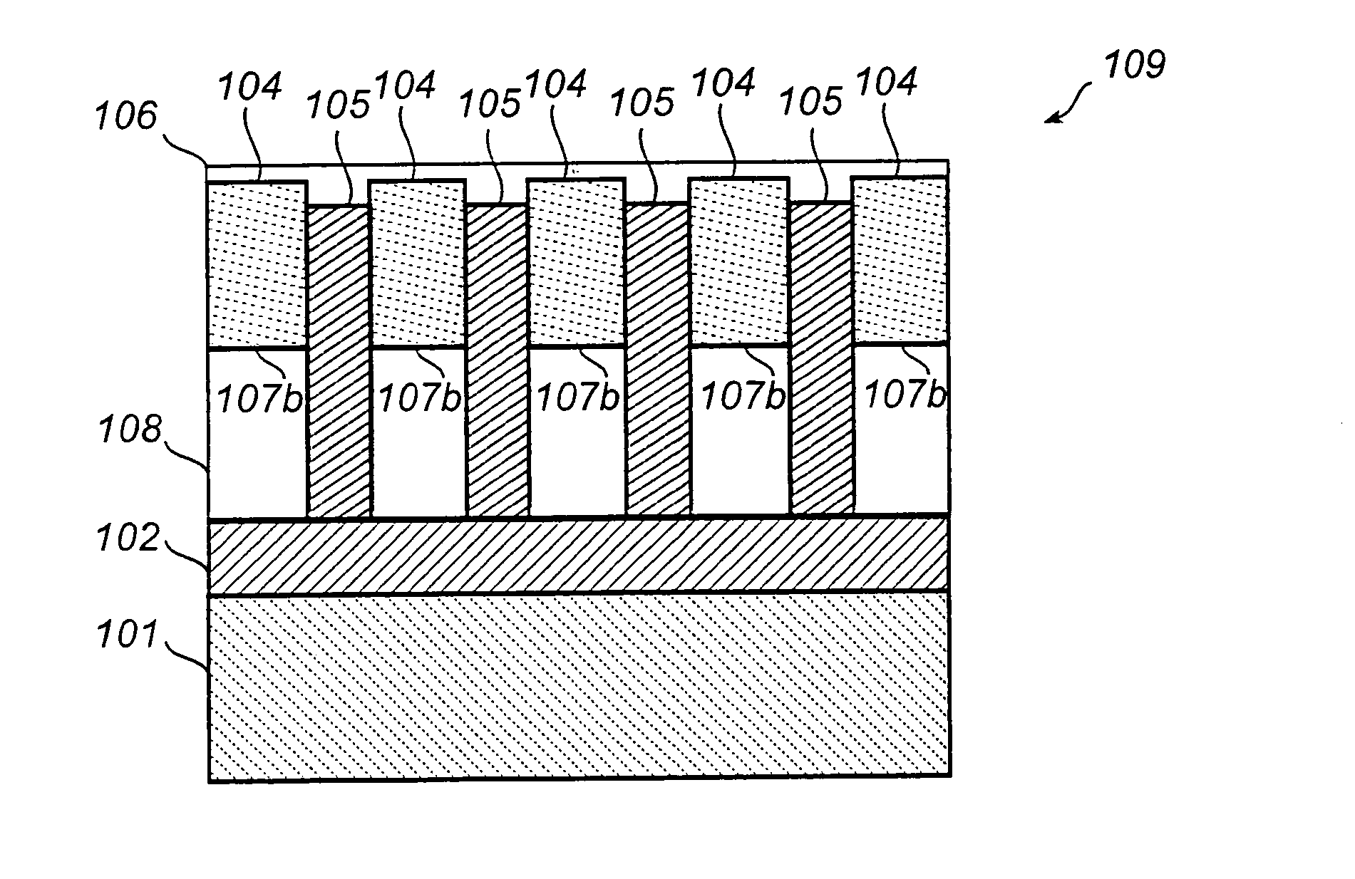
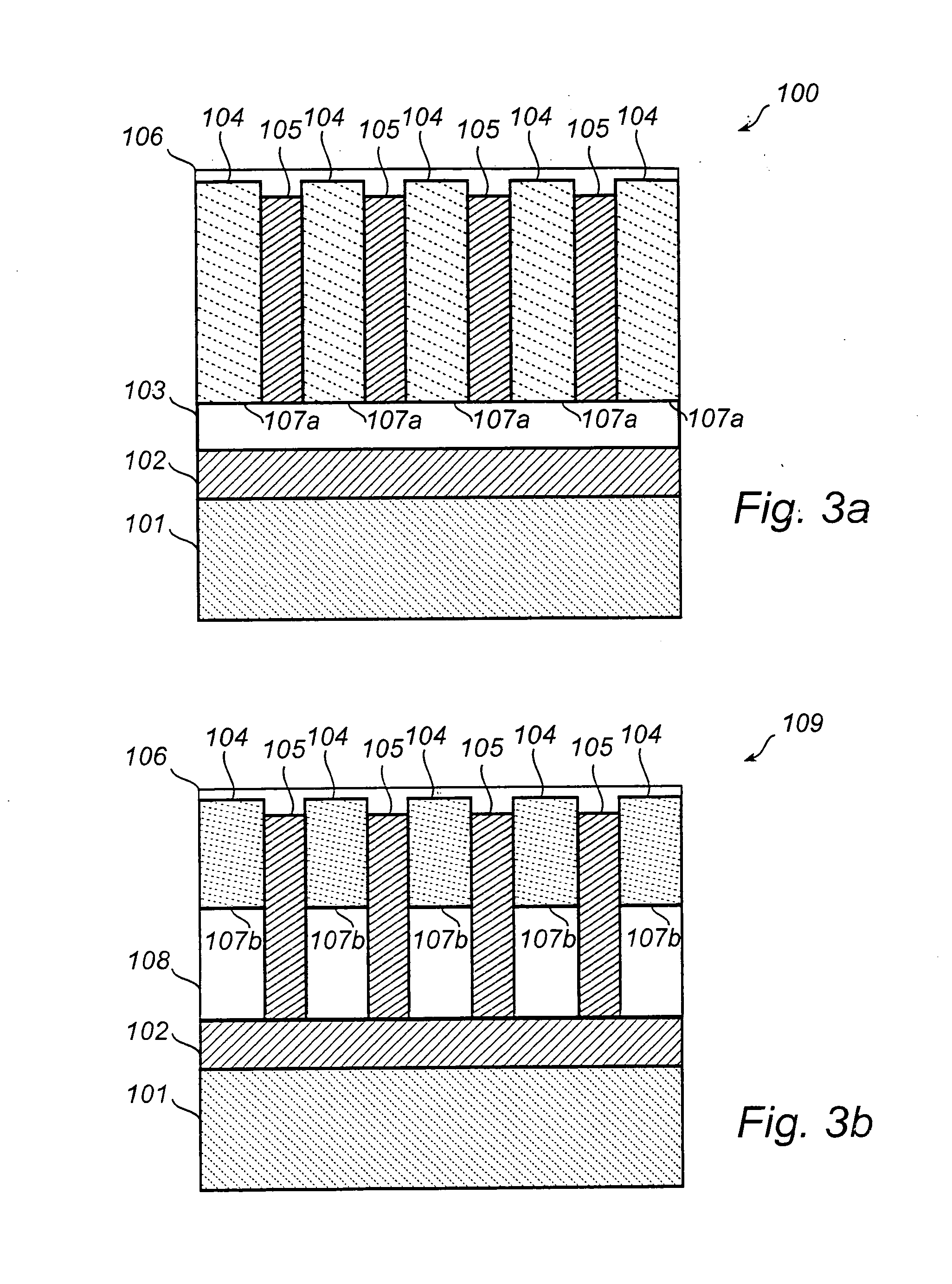
[0029]In FIG. 3a, a currently preferred embodiment of the present invention is shown. A schematic side view illustrates a section of a light-emitting diode (LED) 100 comprising a metallic contact 102 sandwiched between a substrate 101, such as a substrate made of sapphire, and a p-doped layer 103. A plurality of ZnO-nanowires 104 are arranged onto the p-doped layer 103, forming a plurality of p-n junctions 107a. A transparent insulating structure 105 is arranged-among the plurality of ZnO-nanowires ...


PUM


Abstract

The present invention relates to a light emitting diode (100, 109), comprising at least one p-doped structure, a plurality of n-doped zinc-oxide (ZnO) nanowires (104) arranged on the at least one p-doped structure, thereby forming a plurality of p-n junctions (107a, 107b), an insulating structure (105) arranged among the plurality of ZnO-nanowires (104), to electrically separate the plurality of p-n junctions (107a, 107b), and a transparent conductive layer (106), arranged on the at least one insulating structure (105) and in electrical contact with the plurality of ZnO-nanowires (104), to enable application of a voltage over the plurality of p-n junctions (107a, 107b), thereby enabling emission of light. An advantage with the above light emitting diode (100, 109) is its improved broadband spectral distribution. Furthermore, as ZnO-nanowires (104) are used, it is possible to achieve a high brightness.

Description

TECHNICAL FIELD [0001]The present invention relates to a light emitting diode. The present invention also relates to a method for manufacturing such a light emitting diode.TECHNICAL BACKGROUND [0002]Recently, much progress has been made in increasing the brightness of light-emitting diodes (LEDs). As a result, LEDs have become sufficiently bright and inexpensive to serve as light sources in for example general lighting applications.[0003]Commercial high brightness LED-technologies employs so-called thin-film technologies for constructing semiconductors. The materials used for producing high brightness LEDs are selected from the alloys of group III and group V elements in the periodic table. The most widely used semiconductor is Gallium Nitride (GaN) that has a direct band-gap of 3.26 ev.[0004]However, due to disadvantages associated with thin-film technologies, present semiconductor technology seeks to utilize the advantages of nanowires in the areas of LEDs and laser diodes (LDs), ...

Claims


Application Information

Patent Timeline
Patent Type & Authority Applications(United States)
IPC IPC(8): H01L33/00H01L21/20H01L33/08H01L33/18H01L33/28
CPCB82Y20/00H01L33/06H01L33/28H01L33/18H01L33/08
Inventor HU, QIU-HONGWILLANDER, MAGNUSKOUZMINE, VICTOR
Owner ECO SPARK
Learn More